L4960
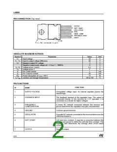
PIN CONNECTION (Top view)
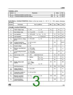
ABSOLUTE MAXIMUM RATINGS
Symbol
Parameter
Value
50
50
-1
Unit
V
V
V1
V1 - V7
V7
Input voltage
Input to output voltage difference
Negative output DC voltage
V
Negative output peak voltage at t = 0.1 s; f = 100KHz
-5
V
µ
V3, V6
V2
Voltage at pin 3 and 6
Voltage at pin 2
5.5
7
V
V
I3
I5
Pin 3 sink current
Pin 5 source current
Power dissipation at Tcase 90 C
1
20
15
mA
mA
W
Ptot
Tj, Tstg
≤
°
Junction and storage temperature
-40 to 150
C
°
PIN FUNCTIONS
FUNCTION
N°
NAME
1
SUPPLY VOLTAGE
FEEDBACK INPUT
Unregulated voltage input. An internal regulator powers the
internal logic.
2
3
The feedback terminal of the regulation loop. The output is
connected directly to this terminal for 5.1V operation; it is
connected via a divider for higher voltages.
FREQUENCY
COMPENSATION
A series RC network connected between this terminal and
ground determines the regulation loop gain characteristics.
4
5
GROUND
Common ground terminal.
OSCILLATOR
A parallel RC network connected to this terminal determines the
switching frequency.
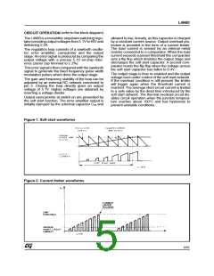
6
SOFT START
OUTPUT
Soft start time constant. A capacitor is connected between this
terminal and ground to define the soft start time constant. This
capacitor also determines the average short circuit output
current.
7
Regulator output.
2/16

 STMICROELECTRONICS [ ST ]