Preliminary
Preliminary
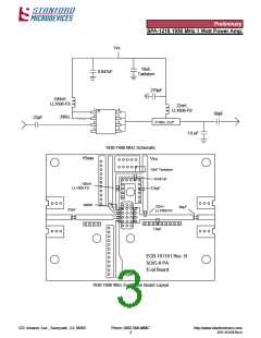
SPA-1218 1950 MHz 1 Watt Power Amp.
Pin # Function
Description
Device Schematic
1
VCC
VCC is the supply voltage for the active bias network.
Bypassing in the appropriate location as shown on
application schematic is required for optimum RF
performance.
2
Vbias
Vbias is the bias control pin for the active bias network.
Device current is set by the current into this pin.
Recommended configuration is shown in the Application
Schematic. Bypassing in the appropriate location as
shown on application schematic is required for optimum
RF performance.
RF input pin. This pin requires the use of an external
DC blocking capacitor chosen for the frequency of
operation.
1
ACTIVE BIAS
2
5-8
NETWORK
3
RF In
N/C
4
5
No connection
3
RF Out/Vcc RF output and bias pin. Bias should be supplied to this
pin through an external RF choke. Because DC biasing
is present on this pin, a DC blocking capacitor should
be used in most applications (see application
schematic). The supply side of the bias network should
be well bypassed. An output matching network is
necessary for optimum performance.
6
7
8
RF Out/Vcc Same as Pin 5
RF Out/Vcc Same as Pin 5
RF Out/Vcc Same as Pin 5
Absolute Maximum Ratings
Parameter
Supply Current (ID)
Value
750
Unit
mA
V
Operation of this device above any one of these
parameters may cause permanent damage.
Device Voltage (VD)
Power Dissipation
Operating Temperature (TOP
RF Input Power
6.0
4.0
W
Bias Conditions should also satisfy the following
expression: IDVD (max) < (TJ - TOP)/Rth,j-l
)
-40 to +85
+500
ºC
mW
ºC
Storage Temperature Range
-40 to +150
+150
Operating Junction Temperature (TJ)
ºC
522 Almanor Ave., Sunnyvale, CA 94085
Phone: (800) SMI-MMIC
http://www.stanfordmicro.com
EDS-101428 Rev A
4

 STANFORD [ STANFORD MICRODEVICES ]