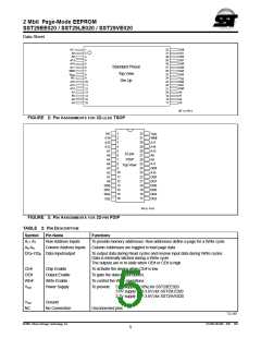
2 Mbit Page-Mode EEPROM
SST29EE020 / SST29LE020 / SST29VE020
Data Sheet
Write Inhibit Mode: Forcing OE# low, CE# high, or WE#
high will inhibit the Write operation. This prevents inadvert-
ent writes during power-up or power-down.
Write Operation Status Detection
The SST29EE/LE/VE020 provide two software means to
detect the completion of a Write cycle, in order to optimize
the system Write cycle time. The software detection
includes two status bits: Data# Polling (DQ7) and Toggle Bit
(DQ6). The end of write detection mode is enabled after the
rising WE# or CE# whichever occurs first, which initiates
the internal Write cycle.
Software Data Protection (SDP)
The SST29EE/LE/VE020 provide the JEDEC approved
optional Software Data Protection scheme for all data alter-
ation operations, i.e., Write and Chip-Erase. With this
scheme, any Write operation requires the inclusion of a
series of three byte-load operations to precede the data
loading operation. The three byte-load sequence is used to
initiate the Write cycle, providing optimal protection from
inadvertent write operations, e.g., during the system power-
up or power-down. The SST29EE/LE/VE020 are shipped
with the Software Data Protection disabled.
The actual completion of the nonvolatile write is asynchro-
nous with the system; therefore, either a Data# Polling or
Toggle Bit read may be simultaneous with the completion
of the Write cycle. If this occurs, the system may possibly
get an erroneous result, i.e., valid data may appear to con-
flict with either DQ7 or DQ6. In order to prevent spurious
rejection, if an erroneous result occurs, the software routine
should include a loop to read the accessed location an
additional two (2) times. If both reads are valid, then the
device has completed the Write cycle, otherwise the rejec-
tion is valid.
The software protection scheme can be enabled by apply-
ing a three-byte sequence to the device, during a page-
load cycle (Figures 5 and 6). The device will then be auto-
matically set into the data protect mode. Any subsequent
Write operation will require the preceding three-byte
sequence. See Table 4 for the specific software command
codes and Figures 5 and 6 for the timing diagrams. To set
the device into the unprotected mode, a six-byte sequence
is required. See Table 4 for the specific codes and Figure 9
for the timing diagram. If a write is attempted while SDP is
enabled the device will be in a non-accessible state for
~300 µs. SST recommends Software Data Protection
always be enabled. See Figure 17 for flowcharts.
Data# Polling (DQ7)
When the SST29EE/LE/VE020 are in the internal Write
cycle, any attempt to read DQ7 of the last byte loaded dur-
ing the byte-load cycle will receive the complement of the
true data. Once the Write cycle is completed, DQ7 will
show true data. The device is then ready for the next opera-
tion. See Figure 7 for Data# Polling timing diagram and Fig-
ure 16 for a flowchart.
The SST29EE/LE/VE020 Software Data Protection is a
global command, protecting all pages in the entire memory
array once enabled (or disabled). Therefore using SDP for
a single Page-Write will enable SDP for the entire array.
Single pages by themselves cannot be SDP enabled or
disabled.
Toggle Bit (DQ6)
During the internal Write cycle, any consecutive attempts to
read DQ6 will produce alternating 0s and 1s, i.e., toggling
between 0 and 1. When the Write cycle is completed, the
toggling will stop. The device is then ready for the next
operation. See Figure 8 for Toggle Bit timing diagram and
Figure 16 for a flowchart. The initial read of the Toggle Bit
will typically be a “1”.
Single power supply reprogrammable nonvolatile memo-
ries may be unintentionally altered. SST strongly recom-
mends that Software Data Protection (SDP) always be
enabled. The SST29EE/LE/VE020 should be programmed
using the SDP command sequence. SST recommends the
SDP Disable Command Sequence not be issued to the
device prior to writing.
Data Protection
The SST29EE/LE/VE020 provide both hardware and soft-
ware features to protect nonvolatile data from inadvertent
writes.
Please refer to the following Application Notes for more
information on using SDP:
•
•
Protecting Against Unintentional Writes When
Using Single Power Supply Flash Memories
Hardware Data Protection
Noise/Glitch Protection: A WE# or CE# pulse of less than 5
ns will not initiate a Write cycle.
The Proper Use of JEDEC Standard Software
Data Protection
VDD Power Up/Down Detection: The Write operation is
inhibited when VDD is less than 2.5V.
©2001 Silicon Storage Technology, Inc.
S71062-06-000 6/01 307
3

 SST [ SILICON STORAGE TECHNOLOGY, INC ]