2 Mbit Page-Mode EEPROM
SST29EE020 / SST29LE020 / SST29VE020
Data Sheet
consists of a specific three-byte load sequence that allows
writing to the selected page and will leave the SST29EE/
LE/VE020 protected at the end of the Page-Write. The
page load cycle consists of loading 1 to 128 Bytes of data
into the page buffer. The internal Write cycle consists of the
TBLCO time-out and the write timer operation. During the
Write operation, the only valid reads are Data# Polling and
Toggle Bit.
Read
The Read operations of the SST29EE/LE/VE020 are con-
trolled by CE# and OE#, both have to be low for the system
to obtain data from the outputs. CE# is used for device
selection. When CE# is high, the chip is deselected and
only standby power is consumed. OE# is the output control
and is used to gate data from the output pins. The data bus
is in high impedance state when either CE# or OE# is high.
Refer to the Read cycle timing diagram for further details
(Figure 4).
The Page-Write operation allows the loading of up to 128
bytes of data into the page buffer of the SST29EE/LE/
VE020 before the initiation of the internal Write cycle. Dur-
ing the internal Write cycle, all the data in the page buffer is
written simultaneously into the memory array. Hence, the
Page-Write feature of SST29EE/LE/VE020 allow the entire
memory to be written in as little as 10 seconds. During the
internal Write cycle, the host is free to perform additional
tasks, such as to fetch data from other locations in the sys-
tem to set up the write to the next page. In each Page-Write
operation, all the bytes that are loaded into the page buffer
must have the same page address, i.e. A7 through A16. Any
byte not loaded with user data will be written to FFH.
Write
The Page-Write to the SST29EE/LE/VE020 should always
use the JEDEC Standard Software Data Protection (SDP)
three-byte command sequence. The SST29EE/LE/VE020
contain the optional JEDEC approved Software Data Pro-
tection scheme. SST recommends that SDP always be
enabled, thus, the description of the write operations will be
given using the SDP enabled format. The three-byte SDP
Enable and SDP Write commands are identical; therefore,
any time a SDP Write command is issued, Software Data
Protection is automatically assured. The first time the three-
byte SDP command is given, the device becomes SDP
enabled. Subsequent issuance of the same command
bypasses the data protection for the page being written. At
the end of the desired Page-Write, the entire device
remains protected. For additional descriptions, please see
the application notes The Proper Use of JEDEC Standard
Software Data Protection and Protecting Against Uninten-
tional Writes When Using Single Power Supply Flash
Memories.
See Figures 5 and 6 for the Page-Write cycle timing dia-
grams. If after the completion of the three-byte SDP load
sequence or the initial byte-load cycle, the host loads a sec-
ond byte into the page buffer within a byte-load cycle time
(TBLC) of 100 µs, the SST29EE/LE/VE020 will stay in the
page load cycle. Additional bytes are then loaded consecu-
tively. The page load cycle will be terminated if no addi-
tional byte is loaded into the page buffer within 200 µs
(TBLCO) from the last byte-load cycle, i.e., no subsequent
WE# or CE# high-to-low transition after the last rising edge
of WE# or CE#. Data in the page buffer can be changed by
a subsequent byte-load cycle. The page load period can
continue indefinitely, as long as the host continues to load
the device within the byte-load cycle time of 100 µs. The
page to be loaded is determined by the page address of
the last byte loaded.
The Write operation consists of three steps. Step 1 is the
three-byte load sequence for Software Data Protection.
Step 2 is the byte-load cycle to a page buffer of the
SST29EE/LE/VE020. Steps 1 and 2 use the same timing
for both operations. Step 3 is an internally controlled Write
cycle for writing the data loaded in the page buffer into the
memory array for nonvolatile storage. During both the SDP
three-byte load sequence and the byte-load cycle, the
addresses are latched by the falling edge of either CE# or
WE#, whichever occurs last. The data is latched by the ris-
ing edge of either CE# or WE#, whichever occurs first. The
internal Write cycle is initiated by the TBLCO timer after the
rising edge of WE# or CE#, whichever occurs first. The
Write cycle, once initiated, will continue to completion, typi-
cally within 5 ms. See Figures 5 and 6 for WE# and CE#
controlled Page-Write cycle timing diagrams and Figures
15 and 17 for flowcharts.
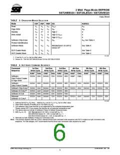
Software Chip-Erase
The SST29EE/LE/VE020 provide a Chip-Erase operation,
which allows the user to simultaneously clear the entire
memory array to the “1” state. This is useful when the entire
device must be quickly erased.
The Software Chip-Erase operation is initiated by using a
specific six-byte load sequence. After the load sequence,
the device enters into an internally timed cycle similar to the
Write cycle. During the Erase operation, the only valid read
is Toggle Bit. See Table 4 for the load sequence, Figure 10
for timing diagram, and Figure 19 for the flowchart.
The Write operation has three functional cycles: the Soft-
ware Data Protection load sequence, the page load cycle,
and the internal Write cycle. The Software Data Protection
©2001 Silicon Storage Technology, Inc.
S71062-06-000 6/01 307
2

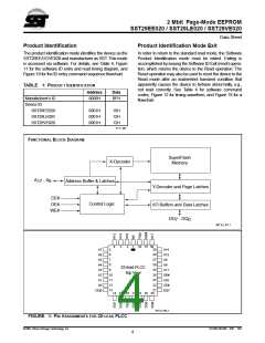
 SST [ SILICON STORAGE TECHNOLOGY, INC ]