4 Mbit SPI Serial Flash
SST25VF040B
Data Sheet
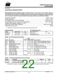
TABLE 10: Capacitance (TA = 25°C, f=1 Mhz, other pins open)
Parameter
Description
Test Condition
VOUT = 0V
Maximum
1
COUT
Output Pin Capacitance
Input Capacitance
12 pF
1
CIN
VIN = 0V
6 pF
T10.0 1295
1. This parameter is measured only for initial qualification and after a design or process change that could affect this parameter.
TABLE 11: Reliability Characteristics
Symbol
Parameter
Endurance
Data Retention
Latch Up
Minimum Specification
Units
Test Method
1
NEND
10,000
100
Cycles JEDEC Standard A117
1
TDR
Years
mA
JEDEC Standard A103
JEDEC Standard 78
1
ILTH
100 + IDD
T11.0 1295
1. This parameter is measured only for initial qualification and after a design or process change that could affect this parameter.
TABLE 12: AC Operating Characteristics
25 MHz
50 MHz
Symbol
Parameter
Serial Clock Frequency
Serial Clock High Time
Serial Clock Low Time
Serial Clock Rise Time (Slew Rate)
Serial Clock Fall Time (Slew Rate)
CE# Active Setup Time
CE# Active Hold Time
CE# Not Active Setup Time
CE# Not Active Hold Time
CE# High Time
Min
Max
Min
Max
Units
MHz
ns
1
FCLK
25
50
TSCKH
TSCKL
18
18
9
9
ns
2
TSCKR
0.1
0.1
10
0.1
0.1
5
V/ns
V/ns
ns
TSCKF
3
TCES
3
TCEH
10
5
ns
3
TCHS
10
5
ns
3
TCHH
10
5
ns
TCPH
TCHZ
TCLZ
TDS
100
50
ns
CE# High to High-Z Output
SCK Low to Low-Z Output
Data In Setup Time
15
8
ns
0
5
0
2
5
5
5
5
5
ns
ns
TDH
THLS
THHS
THLH
THHH
THZ
Data In Hold Time
5
ns
HOLD# Low Setup Time
HOLD# High Setup Time
HOLD# Low Hold Time
HOLD# High Hold Time
HOLD# Low to High-Z Output
HOLD# High to Low-Z Output
Output Hold from SCK Change
Output Valid from SCK
Sector-Erase
10
10
10
10
ns
ns
ns
ns
20
15
8
8
ns
TLZ
ns
TOH
TV
0
0
ns
15
25
25
50
10
8
ns
TSE
25
25
50
10
ms
ms
ms
TBE
Block-Erase
TSCE
TBP
Chip-Erase
Byte-Program
µs
T12.0 1295
1. Maximum clock frequency for Read Instruction, 03H, is 25 MHz
2. Maximum Rise and Fall time may be limited by TSCKH and TSCKL requirements
3. Relative to SCK.
©2007 Silicon Storage Technology, Inc.
S71295-02-000
7/07
23

 SST [ SILICON STORAGE TECHNOLOGY, INC ]