4 Mbit SPI Serial Flash
SST25VF040B
Data Sheet
ELECTRICAL SPECIFICATIONS
Absolute Maximum Stress Ratings (Applied conditions greater than those listed under “Absolute Maximum
Stress Ratings” may cause permanent damage to the device. This is a stress rating only and functional operation
of the device at these conditions or conditions greater than those defined in the operational sections of this data
sheet is not implied. Exposure to absolute maximum stress rating conditions may affect device reliability.)
Temperature Under Bias . . . . . . . . . . . . . . . . . . . . . . . . . . . . . . . . . . . . . . . . . . . . . . . . . . . . . . . . . -55°C to +125°C
Storage Temperature . . . . . . . . . . . . . . . . . . . . . . . . . . . . . . . . . . . . . . . . . . . . . . . . . . . . . . . . . . . . -65°C to +150°C
D. C. Voltage on Any Pin to Ground Potential . . . . . . . . . . . . . . . . . . . . . . . . . . . . . . . . . . . . . . . .-0.5V to VDD+0.5V
Transient Voltage (<20 ns) on Any Pin to Ground Potential . . . . . . . . . . . . . . . . . . . . . . . . . . . . . .-2.0V to VDD+2.0V
Package Power Dissipation Capability (TA = 25°C) . . . . . . . . . . . . . . . . . . . . . . . . . . . . . . . . . . . . . . . . . . . . . . 1.0W
Surface Mount Solder Reflow Temperature . . . . . . . . . . . . . . . . . . . . . . . . . . . . . . . . . . . . . . . 260°C for 10 seconds
Output Short Circuit Current1. . . . . . . . . . . . . . . . . . . . . . . . . . . . . . . . . . . . . . . . . . . . . . . . . . . . . . . . . . . . . . 50 mA
1. Output shorted for no more than one second. No more than one output shorted at a time.
OPERATING RANGE
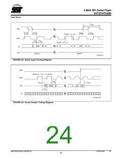
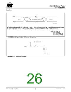
AC CONDITIONS OF TEST
Input Rise/Fall Time . . . . . . . . . . . . . . . 5 ns
Output Load . . . . . . . . . . . . . . . . . . . . . CL = 30 pF
See Figures 26 and 27
Range
Ambient Temp
0°C to +70°C
VDD
Commercial
Industrial
2.7-3.6V
2.7-3.6V
-40°C to +85°C
TABLE 8: DC Operating Characteristics
Limits
Max Units Test Conditions
Symbol Parameter
Min
IDDR
IDDR2
IDDW
ISB
Read Current
10
15
30
20
1
mA
mA
mA
µA
µA
µA
V
CE#=0.1 VDD/0.9 VDD@25 MHz, SO=open
CE#=0.1 VDD/0.9 VDD@50 MHz, SO=open
CE#=VDD
Read Current
Program and Erase Current
Standby Current
CE#=VDD, VIN=VDD or VSS
VIN=GND to VDD, VDD=VDD Max
VOUT=GND to VDD, VDD=VDD Max
VDD=VDD Min
ILI
Input Leakage Current
Output Leakage Current
Input Low Voltage
Input High Voltage
Output Low Voltage
Output Low Voltage
Output High Voltage
ILO
1
VIL
0.8
VIH
0.7 VDD
VDD-0.2
V
VDD=VDD Max
VOL
VOL2
VOH
0.2
0.4
V
IOL=100 µA, VDD=VDD Min
IOL=1.6 mA, VDD=VDD Min
IOH=-100 µA, VDD=VDD Min
V
V
T8.0 1295
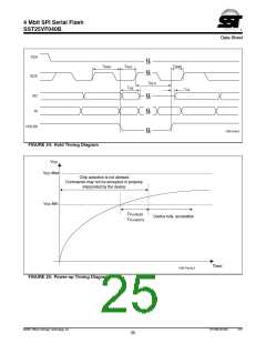
TABLE 9: Recommended System Power-up Timings
Symbol
Parameter
Minimum
Units
1
TPU-READ
VDD Min to Read Operation
VDD Min to Write Operation
10
10
µs
µs
1
TPU-WRITE
T9.0 1295
1. This parameter is measured only for initial qualification and after a design or process change that could affect this parameter.
©2007 Silicon Storage Technology, Inc.
S71295-02-000
7/07
22

 SST [ SILICON STORAGE TECHNOLOGY, INC ]