SFF75N05M
SFF75N05Z
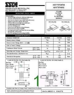
SOLID STATE DEVICES, INC.
14830 Valley View Blvd * La Mirada, Ca 90638
Phone: (562) 404-7855 * Fax: (562) 404-1773
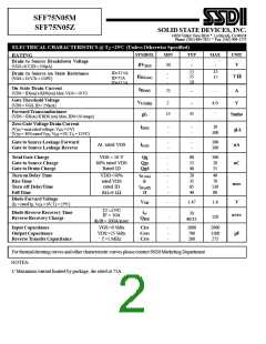
ELECTRICAL CHARACTERISTICS @ T =25oC (Unless Otherwise Specified)
J
SYMBOL
MIN
TYP
MAX
UNIT
V
RATING
Drain to Source Breakdown Voltage
(VGS =0 V, ID = 250µA)
BV
50
-
-
DSS
15
17
13
15
19
-
-
-
ID=37.5A
ID=75A
ID=37.5A
Drain to Source on State Resistance
m Ω
R
(VGS = 10 V,Tc = 150oC)
DS(on)
On State Drain Current
(VDS > ID(on) x RDS(on) Max, VGS = 10 V)
I
D(on)
-
A
-
75
Gate Threshold Voltage
(VDS = VGS, ID = 250µA)
V
2
-
4.0
-
V
GS(th)
Forward Transconductance
(VDS > ID(on) X RDS (on) Max, IDS=20 Amps)
15
35
gf
Smho
s
Zero Gate Voltage Drain Current
-
-
-
-
10
100
I
DSS
(V = max rated voltage, V = 0 V)
DS
GS
µA
(V = 80% rated V , V = 0V, T = 125oC)
DS
DS GS
A
Gate to Source Leakage Forward
Gate to Source Leakage Reverse
-
-
-
-
100
100
At rated VGS
I
GSS
nA
Total Gate Charge
Gate to Source Charge
Gate to Drain Charge
VGS = 10 V
80% rated VDS
Rated ID
Qg
Qgs
Qgd
-
-
-
80
13
40
100
20
55
nC
Turn on Delay Time
Rise Time
Turn off DelayTime
Fall Time
VDD =50%
rated VDS
rated ID
t
-
-
-
-
20
35
65
40
40
70
130
80
d (on)
tr
nsec
t
d (off)
tf
RG=9.1Ω
Diode Forvard Voltage
V
SD
-
1.47
1.6
V
(I = rated I , V = 0V, T = 25oC)
S
D
GS
J
TJ =25oC
IF = 10A
di/dt = 100A/µsec
Diode Reverse Recovery Time
Reverse Recovery Charge
t
rr
70
40/35
nsec
-
150
Q
RR
Input Capacitance
Output Capacitance
Reverse Transfer Capacitance
VGS =0 Volts
VDS =25 Volts
f =1 MHz
Ciss
Coss
Crss
-
-
-
2600
700
260
2900
1100
275
pF
For thermal derating curves and other characteristic curves please contact SSDI Marketing Department.
NOTES:
1/ Maximum current limited by package, die rated at 75A.

 SSDI [ SOLID STATES DEVICES, INC ]