A d v a n c e I n f o r m a t i o n
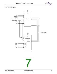
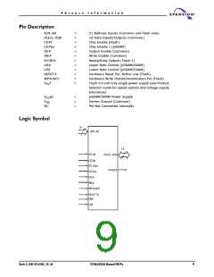
Pin Description
A20–A0
DQ15–DQ0
CE#f
CE#ps
OE#
WE#
RY/BY#
UB#
LB#
RESET#
WP#/ACC
=
=
=
=
=
=
=
=
=
=
=
=
21 Address Inputs (Common and Flash only)
16 Data Inputs/Outputs (Common)
Chip Enable (Flash)
Chip Enable 1 (pSRAM)
Output Enable (Common)
Write Enable (Common)
Ready/Busy Output (Flash 1)
Upper Byte Control (pSRAM/SRAM)
Lower Byte Control (pSRAM/SRAM)
Hardware Reset Pin, Active Low (Flash)
Hardware Write Protect/Acceleration Pin (Flash)
Flash 3.0 volt-only single power supply (see Product
Selector Guide for speed options and voltage supply
tolerances)
VCC
f
VCCps
VSS
NC
=
=
=
pSRAM/SRAM Power Supply
Device Ground (Common)
Pin Not Connected Internally
Logic Symbol
21
A20–A0
16
CE1#f
DQ15–DQ0
R Y/BY#
CE2#f
CE1#ps
CE2ps
OE#
WE#
WP#/ACC
RESET#
UB#
LB#
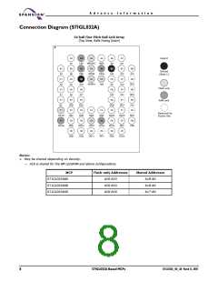
March 31, 2005 S71GL032A_00_A0
S71GL032A Based MCPs
9

 SPANSION [ SPANSION ]