A d v a n c e I n f o r m a t i o n
Contents
Figure 1. Temporary Sector Group Unprotect Operation.......... 35
Figure 2. In-System Sector Group
S71GL032A Based MCPs
Product Selector Guide . . . . . . . . . . . . . . . . . . . . . .4
32 Mb Flash Memory ............................................................................................4
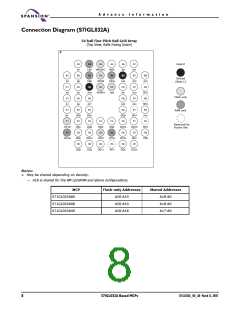
Connection Diagram (S71GL032A) . . . . . . . . . . . . .8
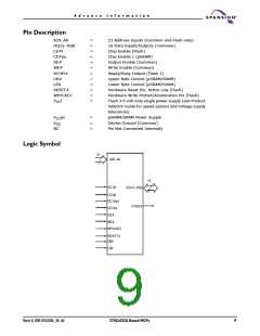
Pin Description . . . . . . . . . . . . . . . . . . . . . . . . . . . . 9
Logic Symbol . . . . . . . . . . . . . . . . . . . . . . . . . . . . . . 9
Ordering Information . . . . . . . . . . . . . . . . . . . . . . . 10
Physical Dimensions . . . . . . . . . . . . . . . . . . . . . . . . 12
TLC056—56-ball Fine-Pitch Ball Grid Array (FBGA)
Protect/Unprotect Algorithms .............................................. 36
Secured Silicon Sector Flash Memory Region ........................................... 37
Write Protect (WP#) .......................................................................................38
Hardware Data Protection .............................................................................38
Low VCC Write Inhibit ................................................................................39
Write Pulse “Glitch” Protection ...............................................................39
Logical Inhibit ...................................................................................................39
Power-Up Write Inhibit ...............................................................................39
Common Flash Memory Interface (CFI) . . . . . . .40
Table 18. CFI Query Identification String .............................. 40
Table 19. System Interface String........................................ 41
Table 20. Device Geometry Definition................................... 42
Table 21. Primary Vendor-Specific Extended Query................ 43
9 x 7 mm Package ............................................................................................... 12
S29GL-A MirrorBit™ Flash Family
General Description . . . . . . . . . . . . . . . . . . . . . . . . 14
Product Selector Guide . . . . . . . . . . . . . . . . . . . . . 16
S29GL064A, S29GL032A .................................................................................. 16
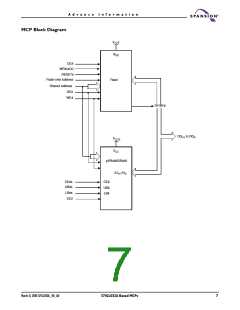
Block Diagram . . . . . . . . . . . . . . . . . . . . . . . . . . . 16
Command Definitions . . . . . . . . . . . . . . . . . . . . . .44
Reading Array Data ...........................................................................................44
Reset Command .................................................................................................44
Autoselect Command Sequence ....................................................................45
Enter Secured Silicon Sector/Exit Secured Silicon
Sector Command Sequence ............................................................................45
Word Program Command Sequence ......................................................45
Unlock Bypass Command Sequence ........................................................46
Write Buffer Programming ..........................................................................46
Accelerated Program ....................................................................................48
Figure 3. Write Buffer Programming Operation ...................... 49
Figure 4. Program Operation............................................... 50
Program Suspend/Program Resume Command Sequence ....................50
Figure 5. Program Suspend/Program Resume........................ 51
Chip Erase Command Sequence ....................................................................51
Sector Erase Command Sequence . . . . . . . . . . . . 53
Figure 6. Erase Operation................................................... 54
Erase Suspend/Erase Resume Commands ..................................................54
Table 22. Command Definitions (x16 Mode) .......................... 56
DQ7: Data# Polling ............................................................................................ 57
Figure 7. Data# Polling Algorithm........................................ 58
RY/BY#: Ready/Busy# .......................................................................................58
Figure 8. Toggle Bit Algorithm............................................. 60
Reading Toggle Bits DQ6/DQ2 ......................................................................61
DQ5: Exceeded Timing Limits .........................................................................61
DQ3: Sector Erase Timer ................................................................................62
DQ1: Write-to-Buffer Abort ...........................................................................62
Table 23. Write Operation Status ......................................... 63
Figure 9. Maximum Negative Overshoot Waveform ................ 64
Figure 10. Maximum Positive
Overshoot Waveform ......................................................... 64
Operating Ranges . . . . . . . . . . . . . . . . . . . . . . . . . .64
DC Characteristics . . . . . . . . . . . . . . . . . . . . . . . . . 65
Test Conditions . . . . . . . . . . . . . . . . . . . . . . . . . . .66
Figure 11. Test Setup......................................................... 66
Table 24. Test Specifications ............................................... 66
Key to Switching Waveforms . . . . . . . . . . . . . . . 66
Figure 12. Input Waveforms and Measurement Levels............ 66
Read-Only Operations-S29GL064A only ....................................................67
Read-Only Operations-S29GL032A only ....................................................67
Figure 13. Read Operation Timings ...................................... 68
Figure 14. Page Read Timings ............................................. 68
Hardware Reset (RESET#) ..............................................................................69
Figure 15. Reset Timings .................................................... 69
Pin Descriptions . . . . . . . . . . . . . . . . . . . . . . . . . . . 17
Logic Symbol-S29GL064A (Model R6, R7) .................................................20
Device Bus Operations . . . . . . . . . . . . . . . . . . . . . . 21
Table 1. Device Bus Operations ........................................... 21
Requirements for Reading Array Data ........................................................ 22
Page Mode Read ............................................................................................. 22
Writing Commands/Command Sequences ................................................ 22
Write Buffer .....................................................................................................23
Accelerated Program Operation ...............................................................23
Autoselect Functions .....................................................................................23
Standby Mode .......................................................................................................23
Automatic Sleep Mode ......................................................................................23
RESET#: Hardware Reset Pin ........................................................................ 24
Output Disable Mode ....................................................................................... 24
Table 2. S29GL032M (Models R1, R2) Sector Addresses ......... 24
Table 3. S29GL032M (Models R3) Top Boot Sector Addresses . 25
Table 4. S29GL032M (Models R4) Bottom
Boot Sector Addresses ....................................................... 25
Table 5. S29GL064A (Models R1, R2, R8, R9)
Sector Addresses .............................................................. 26
Table 6. S29GL064A (Model R3) Top Boot Sector Addresses ... 27
Table 7. S29GL064A (Model R4) Bottom Boot Sector Addresses 28
Table 8. S29GL064A (Model R5) Sector Addresses ................. 29
Table 9. S29GL064A (Models R6, R7) Sector Addresses .......... 30
Autoselect Mode ..................................................................................................31
Sector Group Protection and Unprotection ...............................................31
Table 10. S29GL032A (Models R1, R2) Sector Group Protection/
Unprotection Addresses ...................................................... 32
Table 11. S29GL032A (Models R3) Sector Group Protection/
Unprotection Address Table ................................................ 32
Table 12. S29GL032A (Models R4) Sector Group Protection/
Unprotection Address Table ................................................ 32
Table 13. S29GL064A (Models R1, R2, R8, R9) Sector Group
Protection/Unprotection Addresses ...................................... 32
Table 14. S29GL064A (Model R3) Top Boot Sector Protection/
Unprotection Addresses ...................................................... 34
Table 15. S29GL064A (Model R4) Bottom Boot Sector Protection/
Unprotection Addresses ...................................................... 34
Table 16. S29GL064A (Model R5) Sector Group Protection/
Unprotection Addresses ...................................................... 34
Table 17. S29GL064A (Models R6, R7) Sector Group Protection/
Unprotection Addresses ...................................................... 34
March 31, 2005 S71GL032A_00_A0
S71GL032A Based MCPs
5

 SPANSION [ SPANSION ]