A d v a n c e I n f o r m a t i o n
Product Selector Guide
S29GL064A, S29GL032A
Part Number
S29GL064A
S29GL032A
Speed Option
90
90
90
25
25
10
100
100
30
11
110
110
30
90
90
90
25
25
10
100
100
30
11
110
110
30
Max. Access Time (ns)
Max. CE# Access Time (ns)
Max. Page Access Time (ns)
Max. OE# Access Time (ns)
30
30
30
30
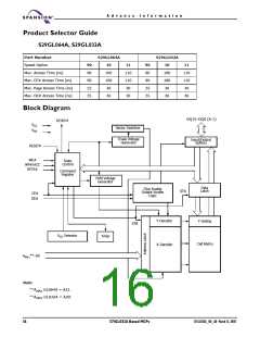
Block Diagram
DQ15–DQ0 (A-1)
RY/BY#
VCC
Sector Switches
VSS
Erase Voltage
Generator
Input/Output
Buffers
RESET#
WE#
WP#/ACC
BYTE#
State
Control
Command
Register
PGM Voltage
Generator
Data
Latch
Chip Enable
Output Enable
Logic
STB
CE#
OE#
Y-Decoder
Y-Gating
STB
VCC Detector
Timer
Cell Matrix
X-Decoder
AMax**–A0
Note:
**A
**A
GL064A = A21.
MAX
GL032A = A20.
MAX
16
S71GL032A Based MCPs
S71GL032A_00_A0 March 31, 2005

 SPANSION [ SPANSION ]