A d v a n c e I n f o r m a t i o n
General Description
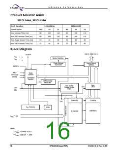
The S29GL-A family of devices are 3.0 V single power Flash memory manufac-
tured using 200 nm MirrorBit technology. The S29GL064A is a 64 Mb, organized
as 4,194,304 words or 8,388,608 bytes. The S29GL032A is a 32 Mb, organized
as 2,097,152 words or 4,194,304 bytes. Depending on the model number, the
devices have an 8-bit wide data bus only, 16-bit wide data bus only, or a 16-bit
wide data bus that can also function as an 8-bit wide data bus by using the BYTE#
input. The devices can be programmed either in the host system or in standard
EPROM programmers.
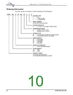
Access times as fast as 90 ns are available. Note that each access time has a spe-
cific operating voltage range (VCC) as specified in the Product Selector Guide and
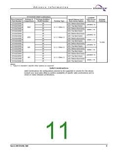
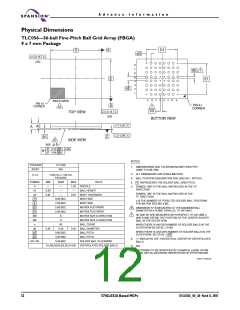
the Ordering Information sections. Package offerings include 48-pin TSOP, 56-pin
TSOP, 48-ball fine-pitch BGA and 64-ball Fortified BGA, depending on model num-
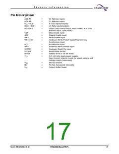
ber. Each device has separate chip enable (CE#), write enable (WE#) and output
enable (OE#) controls.
Each device requires only a single 3.0 volt power supply for both read and
write functions. In addition to a VCC input, a high-voltage accelerated program
(ACC) feature provides shorter programming times through increased current on
the WP#/ACC input. This feature is intended to facilitate factory throughput dur-
ing system production, but may also be used in the field if desired.
The device is entirely command set compatible with the JEDEC single-power-
supply Flash standard. Commands are written to the device using standard mi-
croprocessor write timing. Write cycles also internally latch addresses and data
needed for the programming and erase operations.
The sector erase architecture allows memory sectors to be erased and repro-
grammed without affecting the data contents of other sectors. The device is fully
erased when shipped from the factory.
Device programming and erasure are initiated through command sequences.
Once a program or erase operation has begun, the host system need only poll the
DQ7 (Data# Polling) or DQ6 (toggle) status bits or monitor the Ready/Busy#
(RY/BY#) output to determine whether the operation is complete. To facilitate
programming, an Unlock Bypass mode reduces command sequence overhead
by requiring only two write cycles to program data instead of four.
Hardware data protection measures include a low VCC detector that automat-
ically inhibits write operations during power transitions. The hardware sector
protection feature disables both program and erase operations in any combina-
tion of sectors of memory. This can be achieved in-system or via programming
equipment.
The Erase Suspend/Erase Resume feature allows the host system to pause an
erase operation in a given sector to read or program any other sector and then
complete the erase operation. The Program Suspend/Program Resume fea-
ture enables the host system to pause a program operation in a given sector to
read any other sector and then complete the program operation.
The hardware RESET# pin terminates any operation in progress and resets the
device, after which it is then ready for a new operation. The RESET# pin may be
tied to the system reset circuitry. A system reset would thus also reset the device,
enabling the host system to read boot-up firmware from the Flash memory
device.
14
S71GL032A Based MCPs
S71GL032A_00_A0 March 31, 2005

 SPANSION [ SPANSION ]