A d v a n c e I n f o r m a t i o n
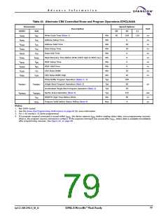
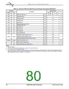
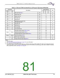
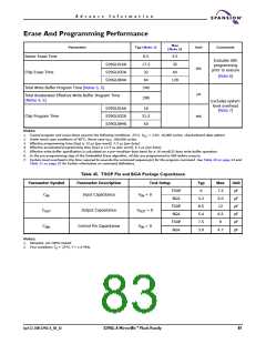
Erase And Programming Performance
Max
(Note 2)
Parameter
Typ (Note 1)
Unit
Comments
Sector Erase Time
Chip Erase Time
0.5
17.5
32
3.5
35
Excludes 00h
programming
prior to erasure
S29GL016A
S29GL032A
S29GL064A
sec
64
(Note 6)
64
128
Total Write Buffer Program Time (Notes 3, 5)
240
µs
Total Accelerated Effective Write Buffer Program Time
(Notes 4, 5)
200
Excludes system
level overhead
(Note 7)
S29GL016A
16
31.5
63
Chip Program Time
S29GL032A
S29GL064A
sec
Notes:
1. Typical program and erase times assume the following conditions: 25°C, V = 3.0V, 10,000 cycles; checkerboard data pattern.
CC
2. Under worst case conditions of 90°C; Worst case V , 100,000 cycles.
CC
3. Effective programming time (typ) is 15 µs (per word), 7.5 µs (per byte).
4. Effective accelerated programming time (typ) is 12.5 µs (per word), 6.3 µs (per byte).
5. Effective write buffer specification is calculated on a per-word/per-byte basis for a 16-word/32-byte write buffer operation.
6. In the pre-programming step of the Embedded Erase algorithm, all bits are programmed to 00h before erasure.
7. System-level overhead is the time required to execute the command sequence(s) for the program command. See Table 30 on page 54 and
Table 31 on page 55 for further information on command definitions.
Table 45. TSOP Pin and BGA Package Capacitance
Parameter Symbol
Parameter Description
Test Setup
Typ
6
Max
7.5
5.0
12
Unit
pF
TSOP
BGA
CIN
Input Capacitance
VIN = 0
4.2
8.5
5.4
7.5
3.9
pF
TSOP
BGA
pF
COUT
Output Capacitance
VOUT = 0
VIN = 0
6.5
9
pF
TSOP
BGA
pF
CIN2
Control Pin Capacitance
4.7
pF
Notes:
1. Sampled, not 100% tested.
2. Test conditions T = 25°C, f = 1.0 MHz.
A
April 22, 2005 S29GL-A_00_A3
S29GL-A MirrorBit™ Flash Family
81

 SPANSION [ SPANSION ]