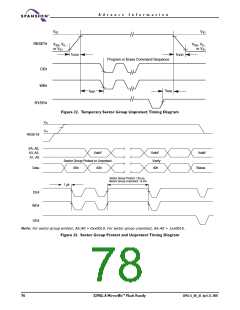
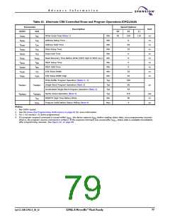
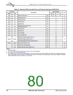
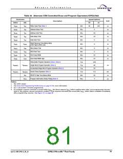
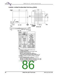
A d v a n c e I n f o r m a t i o n
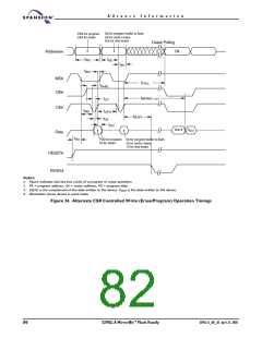
PBA for program
2AA for erase
SA for program buffer to flash
SA for sector erase
555 for chip erase
Data# Polling
Addresses
PA
tWC
tWH
tAS
tAH
WE#
OE#
tPOLL
tGHEL
tWHWH1 or 2
tCP
CE#
Data
tWS
tCPH
tDS
tBUSY
tDH
DQ7#
DOUT
tRH
PBD for program 29 for program buffer to flash
55 for erase
30 for sector erase
10 for chip erase
RESET#
RY/BY#
Notes:
1. Figure indicates last two bus cycles of a program or erase operation.
2. PA = program address, SA = sector address, PD = program data.
3. DQ7# is the complement of the data written to the device. D
4. Illustration shows device in word mode
is the data written to the device.
OUT
Figure 24. Alternate CE# Controlled Write (Erase/Program) Operation Timings
80
S29GL-A MirrorBit™ Flash Family
S29GL-A_00_A3 April 22, 2005

 SPANSION [ SPANSION ]