A d v a n c e I n f o r m a t i o n
Absolute Maximum Ratings
Storage Temperature, Plastic Packages. . . . . . . . . . . . . . . . –65°C to +150°C
Ambient Temperature with Power Applied . . . . . . . . . . . . . . –65°C to +145°C
V
, V (Note 1) . . . . . . . . . . . . . . . . . . . . . . . . . . . . . . . –0.5 V to + 3.0 V
IO
CC
ACC, A9, OE#, and RESET# (Note 2) . . . . . . . . . . . . . . . . .–0.5 V to +13.0 V
Address, Data, Control Signals
(with the exception of CLK) (Note 1) . . . . . . . . . . . . . –0.5 V to 2.75 V
All other pins (Note 1). . . . . . . . . . . . . . . . . . . . . . .–0.5 V to +2.75 V
Output Short Circuit Current (Note 3). . . . . . . . . . . . . . . . . . . . . . . . 200 mA
Notes:
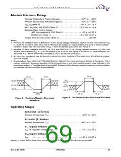
1. Minimum DC voltage on input or I/O pins is –0.5 V. During voltage transitions, input at I/O pins may overshoot VSS
to –2.0 V for periods of up to 20 ns. See 9. Maximum DC voltage on output and I/O pins is 3.0 V. During voltage
transitions output pins may overshoot to VCC + 2.0 V for periods up to 20 ns. See Figure 9.
2. Minimum DC input voltage on pins ACC, A9, OE#, and RESET# is -0.5 V. During voltage transitions, A9, OE#, and
RESET# may overshoot VSS to –2.0 V for periods of up to 20 ns. See Figure 8. Maximum DC input voltage on pin
A9 and OE# is +13.0 V which may overshoot to 14.0 V for periods up to 20 ns.
3. No more than one output may be shorted to ground at a time. Duration of the short circuit should not be greater
than one second.
4. Stresses above those listed under “Absolute Maximum Ratings” may cause permanent damage to the device. This is
a stress rating only; functional operation of the device at these or any other conditions above those indicated in the
operational sections of this data sheet is not implied. Exposure of the device to absolute maximum rating conditions
for extended periods may affect device reliability.
20 ns
20 ns
20 ns
VCC
+2.0 V
+0.8 V
VCC
+0.5 V
–0.5 V
–2.0 V
2.0 V
20 ns
20 ns
20 ns
Figure 9. Maximum Positive Overshoot Waveform
Figure 8. Maximum Negative Overshoot
Waveform
Operating Ranges
Industrial (I) Devices
Ambient Temperature (T ) . . . . . . . . . . . . . . . . . . . . . . . . . –40°C to +85°C
A
Extended (E) Devices
Ambient Temperature (T ) . . . . . . . . . . . . . . . . . . . . . . . . –40°C to +125°C
A
VCC Supply Voltages
V
for regulated voltage range. . . . . . . . . . . . . . . . . . . . . . . 2.5 V to 2.75 V
CC
VIO Supply Voltages
. . . . . . . . . . . . . . . . . . . . . . . . . . . . . . . . . . . . . . . 1.65 V to 2.75 V
Operating ranges define those limits between which the functionality of the device is guaranteed.
V
IO
March 22, 2004 30606B0
S29CD032G
69

 SPANSION [ SPANSION ]