A d v a n c e I n f o r m a t i o n
Table Of Contents
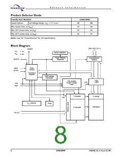
Product Selector Guide. . . . . . . . . . . . . . . . . . . . . . 6
Block Diagram . . . . . . . . . . . . . . . . . . . . . . . . . . . . . 6
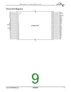
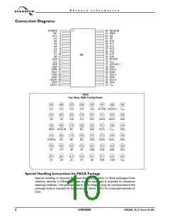
Connection Diagrams . . . . . . . . . . . . . . . . . . . . . . . 7
Special Handling Instructions for FBGA Package ..........................8
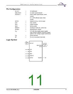
Pin Configuration. . . . . . . . . . . . . . . . . . . . . . . . . . . 9
Logic Symbol . . . . . . . . . . . . . . . . . . . . . . . . . . . . . . 9
Ordering Information . . . . . . . . . . . . . . . . . . . . . . 10
Standard Products .................................................................................10
Device Bus Operations . . . . . . . . . . . . . . . . . . . . . . 11
Table 1. S29AL004D Device Bus Operations .........................11
Word/Byte Configuration ....................................................................11
Requirements for Reading Array Data ............................................11
Writing Commands/Command Sequences ................................... 12
Program and Erase Operation Status .............................................. 12
Standby Mode ......................................................................................... 12
Automatic Sleep Mode ......................................................................... 13
RESET#: Hardware Reset Pin ............................................................ 13
Output Disable Mode ........................................................................... 13
Table 2. S29AL004D Top Boot Block Sector Addresses ...........13
Table 3. S29AL004D Bottom Boot Block Sector Addresses ......14
Autoselect Mode ...................................................................................14
Table 4. S29AL004D Autoselect Codes
(High Voltage Method) .......................................................15
Sector Protection/Unprotection ....................................................... 15
Temporary Sector Unprotect ........................................................... 15
Figure 1. Temporary Sector Unprotect Operation................... 16
Figure 2. In-System Sector Protect/Sector Unprotect
DQ2: Toggle Bit II ................................................................................28
Reading Toggle Bits DQ6/DQ2 ....................................................... 29
DQ5: Exceeded Timing Limits .......................................................... 29
DQ3: Sector Erase Timer .................................................................. 29
Figure 6. Toggle Bit Algorithm............................................ 30
Table 6. Write Operation Status ......................................... 31
Absolute Maximum Ratings . . . . . . . . . . . . . . . . . 32
Operating Ranges. . . . . . . . . . . . . . . . . . . . . . . . . . 32
Industrial (I) Devices ............................................................................32
VCC Supply Voltages .............................................................................32
DC Characteristics. . . . . . . . . . . . . . . . . . . . . . . . . 33
Figure 7. Maximum Negative Overshoot Waveform ............... 33
Figure 8. Maximum Positive Overshoot Waveform................. 33
Table 7. CMOS Compatible ................................................ 33
Figure 9. ICC1 Current vs. Time (Showing Active and
Automatic Sleep Currents)................................................. 34
Figure 10. Typical ICC1 vs. Frequency.................................. 34
Test Conditions . . . . . . . . . . . . . . . . . . . . . . . . . . . 35
Figure 11. Test Setup ....................................................... 35
Table 8. Test Specifications ............................................... 35
Key to Switching Waveforms . . . . . . . . . . . . . . . . 36
Figure 12. Input Waveforms and Measurement Levels........... 36
AC Characteristics . . . . . . . . . . . . . . . . . . . . . . . . . 37
Table 9. Read Operations .................................................. 37
Figure 13. Read Operations Timings.................................... 37
Table 10. Hardware Reset (RESET#) ................................... 38
Figure 14. RESET# Timings ............................................... 38
Table 11. Word/Byte Configuration (BYTE#) ........................ 39
Figure 15. BYTE# Timings for Read Operations..................... 40
Figure 16. BYTE# Timings for Write Operations .................... 40
Table 12. Erase/Program Operations ................................... 41
Figure 17. Program Operation Timings ................................ 42
Figure 18. Chip/Sector Erase Operation Timings ................... 43
Figure 19. Data# Polling Timings (During Embedded
Algorithms....................................................................... 17
Hardware Data Protection .................................................................18
Low VCC Write Inhibit ........................................................................18
Write Pulse Glitch Protection ...........................................................18
Logical Inhibit ..........................................................................................18
Power-Up Write Inhibit ......................................................................18
Command Definitions . . . . . . . . . . . . . . . . . . . . . . 18
Reading Array Data ..............................................................................18
Reset Command ....................................................................................19
Autoselect Command Sequence .......................................................19
Word/Byte Program Command Sequence ....................................19
Algorithms)..................................................................... 44
Figure 20. Toggle Bit Timings (During Embedded
Algorithms)..................................................................... 44
Figure 21. DQ2 vs. DQ6 .................................................... 45
Table 13. Temporary Sector Unprotect ................................ 45
Figure 22. Temporary Sector Unprotect Timing Diagram........ 45
Figure 23. Sector Protect/Unprotect Timing Diagram............. 46
Table 14. Alternate CE# Controlled Erase/Program
Unlock Bypass Command Sequence ...............................................20
Figure 3. Program Operation .............................................. 21
Chip Erase Command Sequence .......................................................21
Operation ........................................................................ 47
Figure 24. Alternate CE# Controlled Write Operation
Timings .......................................................................... 48
Table 15. Erase And Programming Performance .................... 48
Table 16. TSOP, SO, And BGA Pin Capacitance ..................... 49
Sector Erase Command Sequence ..................................................22
Erase Suspend/Erase Resume Commands ....................................22
Figure 4. Erase Operation .................................................. 24
Table 5. S29AL004D Command Definitions ...........................24
Physical Dimensions. . . . . . . . . . . . . . . . . . . . . . . . 50
TS 048—48-Pin Standard TSOP .................................................... 50
VBK 048 - 48 Ball Fine-Pitch Ball Grid Array
Write Operation Status . . . . . . . . . . . . . . . . . . . . 26
(FBGA) 8.15 x 6.15 mm ..........................................................................51
SO 044—44-Pin Small Outline Package ........................................52
Revision Summary . . . . . . . . . . . . . . . . . . . . . . . . . 53
DQ7: Data# Polling ..............................................................................26
Figure 5. Data# Polling Algorithm ....................................... 27
RY/BY#: Ready/Busy# ......................................................................... 27
DQ6: Toggle Bit I ..................................................................................28
February 18, 2005 S29AL004D_00_A1
S29AL004D
5

 SPANSION [ SPANSION ]