A d v a n c e I n f o r m a t i o n
General Description
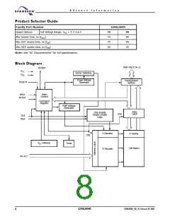
The S29AL004D is a 4 Mbit, 3.0 volt-only Flash memory organized as 524,288
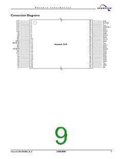
bytes or 262,144 words. The device is offered in 48-ball FBGA, 44-pin SO, and
48-pin TSOP packages. The word-wide data (x16) appears on DQ15–DQ0; the
byte-wide (x8) data appears on DQ7–DQ0. This device requires only a single, 3.0
volt V
supply to perform read, program, and erase operations. A standard
CC
EPROM programmer can also be used to program and erase the device.
This device is manufactured using Spansion’s 200nm process technology, and of-
fers all the features and benefits of the Am29LV400B and MBM29LV400T/BC,
which were manufactured using 320nm process technology.
The standard device offers access times of 70 and 90ns, allowing high speed mi-
croprocessors to operate without wait states. To eliminate bus contention the
device has separate chip enable (CE#), write enable (WE#) and output enable
(OE#) controls.
The device requires only a single 3.0 volt power supply for both read and write
functions. Internally generated and regulated voltages are provided for the pro-
gram and erase operations.
The device is entirely command set compatible with the JEDEC single-power-
supply Flash standard. Commands are written to the command register using
standard microprocessor write timings. Register contents serve as input to an in-
ternal state-machine that controls the erase and programming circuitry. Write
cycles also internally latch addresses and data needed for the programming and
erase operations. Reading data out of the device is similar to reading from other
Flash or EPROM devices.
Device programming occurs by executing the program command sequence. This
initiates the Embedded Program algorithm—an internal algorithm that auto-
matically times the program pulse widths and verifies proper cell margin. The
Unlock Bypass mode facilitates faster programming times by requiring only two
write cycles to program data instead of four.
Device erasure occurs by executing the erase command sequence. This initiates
the Embedded Erase algorithm—an internal algorithm that automatically
preprograms the array (if it is not already programmed) before executing the
erase operation. During erase, the device automatically times the erase pulse
widths and verifies proper cell margin.
The host system can detect whether a program or erase operation is complete by
observing the RY/BY# pin, or by reading the DQ7 (Data# Polling) and DQ6 (tog-
gle) status bits. After a program or erase cycle is completed, the device is ready
to read array data or accept another command.
The sector erase architecture allows memory sectors to be erased and repro-
grammed without affecting the data contents of other sectors. The device is fully
erased when shipped from the factory.
Hardware data protection measures include a low V detector that automat-
CC
ically inhibits write operations during power transitions. The hardware sector
protection feature disables both program and erase operations in any combina-
tion of the sectors of memory. This can be achieved in-system or via
programming equipment.
February 18, 2005 S29AL004D_00_A1
S29AL004D
3

 SPANSION [ SPANSION ]