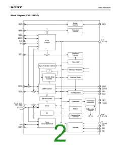
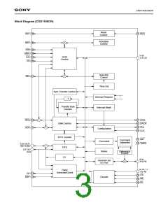
CXD1185CQ/CR
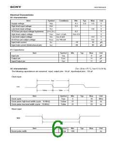
Electrical Characteristics
DC characteristics
Item
Symbol
VDD
Conditions
Min.
4.5
Typ.
5.0
Max.
Unit
V
Supply voltage
5.5
High level input voltage
Low level input voltage
SCSI bus pin input voltage hysteresis
High level output voltage
Low level output voltage
SCSI bus pin output voltage
Input leak current
VIHT
2.2
V
VILT
0.8
V
(VT+)–(VT–)
VOH
0.2
V
IOH=–2 mA
VDD–0.5
V
VOL
IOL=4 mA
0.4
0.5
10
V
VOLS
ILI1
IOL=48 mA
V
–10
–40
µA
µA
Input leak current (bidirectional pin)
ILI2
40
I/O Capacitance
Item
Symbol
CIN
Min.
Typ.
Max.
9
Unit
pF
Input pin
Output pin
COUT
CI/O
11
pF
Input/Output pin
11
pF
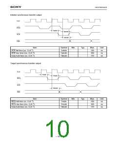
AC characteristics
(Ta=–20 to +75 °C, VDD=5 V±10 %)
The following capacitances are assumed : input, output pins : 65 pF, input/output pins : 125 pF
Clock input
Tcyc
CLK
Tcklw
Tckhw
Item
Symbol
Min.
5
Typ.
Max.
16
Unit
MHz
ns
Clock cycle
Tcyc
Tcknw
Tcklw
Clock pulse high level width (cycle : 16 MHz)
Clock pulse low level width (cycle : 16 MHz)
31
31
33
33
ns
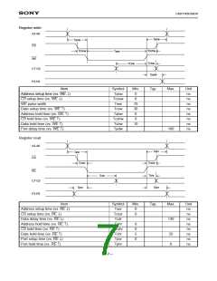
Reset input
RES
Tresw
Item
Symbol
Tresw
Min.
100
Typ.
Max.
Unit
ns
Reset pulse width
—6—

 SONY [ SONY CORPORATION ]