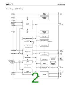
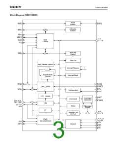
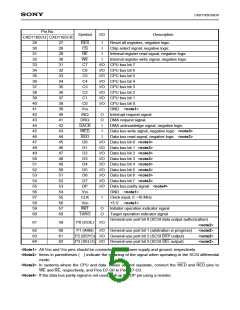
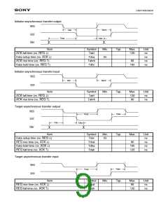
CXD1185CQ/CR
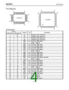
Pin No.
Symbol
I/O
Description
CXD1185CQ CXD1185CR
29
30
31
32
33
34
35
36
37
38
39
40
41
42
43
44
45
46
47
48
49
50
51
52
53
54
55
56
57
58
59
60
27
28
29
30
31
32
33
34
35
36
37
38
39
40
41
42
43
44
45
46
47
48
49
50
51
52
53
54
55
56
57
58
RES
CS
I
I
I
I
Reset all registers, negative logic
Chip select signal, negative logic
RE
Internal register read signal, negative logic
Internal register write signal, negative logic
WE
C7
I/O CPU bus bit 7
I/O CPU bus bit 6
I/O CPU bus bit 5
I/O CPU bus bit 4
I/O CPU bus bit 3
I/O CPU bus bit 2
I/O CPU bus bit 1
I/O CPU bus bit 0
GND <note1>
C6
C5
C4
C3
C2
C1
C0
VSS
IRQ
DRQ
DACK
WED
RED
D0
O
O
I
Interrupt request signal
DMA request signal
DMA acknowledge signal, negative logic
Data bus write signal, negative logic <note3>
Data bus read signal, negative logic <note3>
I
I
I/O Data bus bit 0 <note3>
I/O Data bus bit 1 <note3>
I/O Data bus bit 2 <note3>
I/O Data bus bit 3 <note3>
I/O Data bus bit 4 <note3>
I/O Data bus bit 5 <note3>
I/O Data bus bit 6 <note3>
I/O Data bus bit 7 <note3>
I/O Data bus parity signal <note4>
GND <note1>
D1
D2
D3
D4
D5
D6
D7
DP
VSS
CLK
VDD
INIT
TARG
I
Clock input, 5 –16 MHz
+5 V <note1>
O
O
Initiator operation indicator signal
Target operation indicator signal
General-use port bit 0 (SCSI data output authorization)
<note2>
61
59
P0 (DOE) I/O
62
63
64
60
61
62
P1 (ARB) I/O General-use port bit 1 (arbitration in progress)
P2 (BSYO) I/O General-use port bit 2 (SCSI BSY output)
P3 (SELO) I/O General-use port bit 3 (SCSI SEL output)
<note2>
<note2>
<note2>
<Note1> All VDD and VSS pins should be connected to the power supply and ground, respectively.
<Note2> Items in parentheses ( ) indicate the meaning of the signal when operating in the SCSI differential
mode.
<Note3> In systems where the CPU and data buses are not separate, connect the WED and RED pins to
WE and RE, respectively, and Pins D7-D0 to Pins C7-C0.
<Note4> If the data bus parity signal is not used, pull up the DP pin using a resistor.
—5—

 SONY [ SONY CORPORATION ]