TABLE OF CONTENTS
1.0 GENERAL DESCRIPTION.................................................................................................................................. 6
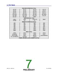
2.0 PIN TABLE.......................................................................................................................................................... 7
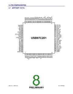
3.0 PIN CONFIGURATION........................................................................................................................................ 8
3.1
QFP/TQFP 100 Pin..........................................................................................................................8
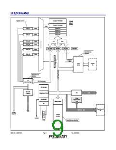
4.0 BLOCK DIAGRAM .............................................................................................................................................. 9
5.0 PIN DESCRIPTIONS......................................................................................................................................... 10
5.1
6.0 FUNCTIONAL BLOCK DESCRIPTIONS .......................................................................................................... 14
6.1
6.1.1
BUFFER TYPE DESCRIPTIONS...................................................................................................13
MCU ...............................................................................................................................................14
MCU Memory Map: Code Space...........................................................................................14
MCU Memory Map: XData Space..........................................................................................15
MCU Block Register Summary..............................................................................................16
MCU Register Descriptions....................................................................................................19
SIE Block .......................................................................................................................................42
Autonomous USB Protocol....................................................................................................42
USB Events............................................................................................................................43
Standard Device Requests ....................................................................................................44
SIE Configurations.................................................................................................................44
IDE Controller Description...........................................................................................................44
IDE Configurations.................................................................................................................45
PIO IDE Operations ...............................................................................................................45
PIO IDE Data Prefetching and Posting..................................................................................45
DMA Transfers.......................................................................................................................46
Ultra ATA/66 Synchronous DMA Operation...........................................................................46
Ultra ATA/66 Operation..........................................................................................................47
SRAM Buffers................................................................................................................................48
8051 Options.................................................................................................................................48
Address Multiplexing ...................................................................................................................48
SRAM Time Multiplexer Operation .............................................................................................49
Phase 0 (Ø0)..........................................................................................................................49
Phase 1 (Ø1)..........................................................................................................................49
Phase 2 (Ø2)..........................................................................................................................49
Phase 3 (Ø3)..........................................................................................................................49
EP2 SRAM Buffer Operation........................................................................................................49
EP2 Automatic Buffer Operations...............................................................................................50
Receive Auto-Toggle .............................................................................................................50
Transmit Buffer Operation .....................................................................................................51
Automatic Transfer Operation................................................................................................52
6.1.2
6.1.3
6.1.4
6.2
6.2.1
6.2.2
6.2.3
6.2.4
6.3
6.3.1
6.3.2
6.3.3
6.3.4
6.3.5
6.3.6
6.4
6.5
6.6
6.7
6.7.1
6.7.2
6.7.3
6.7.4
6.8
6.9
6.9.1
6.9.2
6.9.3
7.0 DC PARAMETERS............................................................................................................................................ 54
8.0 AC SPECIFICATIONS....................................................................................................................................... 56
8.1
8.2
ATA/ATAPI.....................................................................................................................................56
USB2.0 Timing ..............................................................................................................................56
9.0 PACKAGING ..................................................................................................................................................... 57
10.0 USB97C201 REVISIONS.............................................................................................................................. 59
SMSC DS – USB97C201
Page 3
Rev. 03/25/2002
PRELIMINARY

 SMSC [ SMSC CORPORATION ]