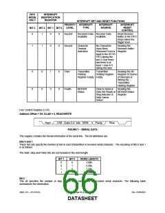
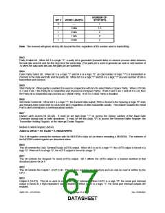
NUMBER OF
STOP BITS
BIT 2
WORD LENGTH
0
1
1
1
1
--
1
1.5
2
5 bits
6 bits
7 bits
8 bits
2
2
Note: The receiver will ignore all stop bits beyond the first, regardless of the number used in transmitting.
Bit 3
Parity Enable bit. When bit 3 is a logic "1", a parity bit is generated (transmit data) or checked (receive data) between
the last data word bit and the first stop bit of the serial data. (The parity bit is used to generate an even or odd number of
1s when the data word bits and the parity bit are summed).
Bit 4
Even Parity Select bit. When bit 3 is a logic "1" and bit 4 is a logic "0", an odd number of logic "1"'s is transmitted or
checked in the data word bits and the parity bit. When bit 3 is a logic "1" and bit 4 is a logic "1" an even number of bits is
transmitted and checked.
Bit 5
Stick Parity bit. When parity is enabled it is used in conjunction with bit 4 to select Mark or Space Parity. When LCR bits
3, 4 and 5 are 1 the Parity bit is transmitted and checked as 0 (Space Parity). If bits 3 and 5 are 1 and bit 4 is a 0, then
the Parity bit is transmitted and checked as 1 (Mark Parity). If bit 5 is 0 Stick Parity is disabled.
Bit 6
Set Break Control bit. When bit 6 is a logic "1", the transmit data output (TXD) is forced to the Spacing or logic "0" state
and remains there (until reset by a low level bit 6) regardless of other transmitter activity. This feature enables the Serial
Port to alert a terminal in a communications system.
Bit 7
Divisor Latch Access bit (DLAB). It must be set high (logic "1") to access the Divisor Latches of the Baud Rate
Generator during read or write operations. It must be set low (logic "0") to access the Receiver Buffer Register, the
Transmitter Holding Register, or the Interrupt Enable Register.
Modem Control Register (MCR)
Address Offset = 4H, DLAB = X, READ/WRITE
This 8 bit register controls the interface with the MODEM or data set (or device emulating a MODEM). The contents of
the MODEM control register are described below.
Bit 0
This bit controls the Data Terminal Ready (nDTR) output. When bit 0 is set to a logic "1", the nDTR output is forced to a
logic "0". When bit 0 is a logic "0", the nDTR output is forced to a logic "1".
Bit 1
This bit controls the Request To Send (nRTS) output. Bit 1 affects the nRTS output in a manner identical to that
described above for bit 0.
Bit 2
This bit controls the Output 1 (OUT1) bit. This bit does not have an output pin and can only be read or written by the
CPU.
Bit 3
Output 2 (OUT2). This bit is used to enable an UART interrupt. When OUT2 is a logic "0", the serial port interrupt
output is forced to a high impedance state - disabled. When OUT2 is a logic "1", the serial port interrupt outputs are
enabled.
SMSC DS – LPC47S45x
Page 67 of 259
Rev. 07/09/2001
DATASHEET

 SMSC [ SMSC CORPORATION ]