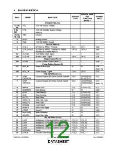
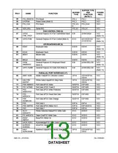
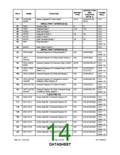
BUFFER TYPE
PER
FUNCTION
(NOTE 1)
BUFFER
TYPE
POWER
WELL
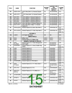
PIN #
NAME
FUNCTION
50
51
52
53
64
65
GP26
/SYSOPT
General Purpose I/O /SYSOPT (Note 7)
General Purpose I/O /LED1 (Note 9)
General Purpose I/O /LED2 (Note 9)
General Purpose I/O /IO_SMI#
IO8
(I/O8/OD8)
VCC
(Note 13)
VCC
(Note 13)
VCC
GP60 /LED1
IO12
IO12
IO12
IO8
(I/O12/OD12)/
(O12/OD12)
(I/O12/OD12)/
(O12/OD12)
GP61 /LED2
(Note 13)
VCC
GP27
/IO_SMI#
(I/O12/OD12)/
(O12/OD12)
(Note 13)
VCC
GP34
/IRQINA
General Purpose I/O / IRQ Input A
General Purpose I/O / IRQ Input B
(I/O8/OD8)/I
(Note 13)
VCC
GP35
IO8
(I/O8/OD8)/I
/IRQINB
(Note 13)
Note: The "n" as the first letter of a signal name or the “#” as the suffix of a signal name indicates an "Active Low"
signal.
Note 1: Buffer types per function on multiplexed pins are separated by a slash “/”. Buffer types in parenthesis
represent multiple buffer types for a single pin function.
Note 2: The LPCPD# pin may be tied high. The LPC interface will function properly if the PCI_RESET# signal
follows the protocol defined for the LRESET# signal in the “Low Pin Count Interface Specification”.
Note 3: If the 32kHz input clock is not used and the crystal is not connected, a bit in the configuration register at 0xF0
in
Logical Device A, which indicates whether or not the 32KHz clock is connected, should be set to ‘1’. This bit
determines the clock source for the fan tachometer, LED and “wake on specific key” logic. CLKI32 pin MUST not be
grounded if XOSEL is left unconnected.
Note 4: The fan control pin (FAN) comes up as output and low following a VCC POR and PCI Reset (also known as a
Hard Reset). This pin reverts to its non-inverting GPIO input function when VCC is removed from the part.
Note 5: The GP53/TXD2/IRTX pin is an output and low when the part is under VTR power (VCC=0). The pin comes
up as output and low following a VCC POR and PCI Reset.
Note 6: VTR can be connected to VCC if no wakeup functionality is required.
Note 7: The GP35/IRQINB/SYSOPT pin requires an external pulldown resistor to put the base I/O address for
configuration at 0x02E. An external pullup resistor is required to move the base I/O address for configuration to
0x04E.
Note 8: External pullups must be placed on the nKBDRST and A20M pins. These pins are GPIOs that
are inputs after an initial power-up (VTR POR). If the nKBDRST and A20M functions are to be used, the system
must ensure that these pins are high. See Section “Pins That Require External Pullup Resistor”.
Note 9: The LED pins are powered by VTR so that the LEDs can be controlled when the part is under VTR power.
The GP61 pin defaults to the LED function active (blinking at a 1 Hz rate, 50% duty cycle) on initial power up (as long
as the 32 kHz clock input is active or crystal is connected).
Note 10: External pullups are required on the XRD# and XWR# pins.
Note 11: XCS1is an active high signal and is designed to be used with supported LCD controllers.
Note 12: When XOSEL = ‘0’, the RTC uses a 32.768kHz crystal connected between the XTAL1 and XTAL2 pins.
When XOSEL = ‘1’, the RTC is driven by a 32.768kHz single-ended clock source connected to the XTAL2 pin.
Note 13: These pins have input buffers into the wakeup logic that are powered by VTR.
SMSC DS – LPC47S45x
Page 16 of 259
Rev. 07/09/2001
DATASHEET

 SMSC [ SMSC CORPORATION ]