BIT 5 PE - PAPER END
The level on the PE input is read by the CPU as bit 5 of the Printer Status Register. A logic 1 indicates a paper end; a
logic 0 indicates the presence of paper.
BIT 6 nACK - ACKNOWLEDGE
The level on the nACK input is read by the CPU as bit 6 of the Printer Status Register. A logic 0 means that the printer
has received a character and can now accept another. A logic 1 means that it is still processing the last character or has
not received the data.
BIT 7 nBUSY - nBUSY
The complement of the level on the BUSY input is read by the CPU as bit 7 of the Printer Status Register. A logic 0 in
this bit means that the printer is busy and cannot accept a new character. A logic 1 means that it is ready to accept the
next character.
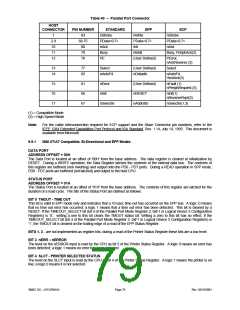
CONTROL PORT
ADDRESS OFFSET = 02H
The Control Port is located at an offset of '02H' from the base address. The Control Register is initialized by the RESET
input, bits 0 to 5 only being affected; bits 6 and 7 are hard wired low.
BIT 0 STROBE - STROBE
This bit is inverted and output onto the nSTROBE output.
BIT 1 AUTOFD - AUTOFEED
This bit is inverted and output onto the nAutoFd output. A logic 1 causes the printer to generate a line feed after each
line is printed. A logic 0 means no autofeed.
BIT 2 nINIT - INITIATE OUTPUT
This bit is output onto the nINIT output without inversion.
BIT 3 SLCTIN - PRINTER SELECT INPUT
This bit is inverted and output onto the nSLCTIN output. A logic 1 on this bit selects the printer; a logic 0 means the
printer is not selected.
BIT 4 IRQE - INTERRUPT REQUEST ENABLE
The interrupt request enable bit when set to a high level may be used to enable interrupt requests from the Parallel Port
to the CPU. An interrupt request is generated on the IRQ port by a positive going nACK input. When the IRQE bit is
programmed low the IRQ is disabled.
BIT 5 PCD - PARALLEL CONTROL DIRECTION
Parallel Control Direction is not valid in printer mode. In printer mode, the direction is always out regardless of the state
of this bit. In bi-directional, EPP or ECP mode, a logic 0 means that the printer port is in output mode (write); a logic 1
means that the printer port is in input mode (read).
Bits 6 and 7 during a read are a low level, and cannot be written.
EPP ADDRESS PORT
ADDRESS OFFSET = 03H
The EPP Address Port is located at an offset of '03H' from the base address. The address register is cleared at
initialization by RESET. During a WRITE operation, the contents of the internal data bus DB0-DB7 are buffered (non
inverting) and output onto the PD0 - PD7 ports. An LPC I/O write cycle causes an EPP ADDRESS WRITE cycle to be
performed, during which the data is latched for the duration of the EPP write cycle. During a READ operation, PD0 -
PD7 ports are read. An LPC I/O read cycle causes an EPP ADDRESS READ cycle to be performed and the data
output to the host CPU, the deassertion of ADDRSTB latches the PData for the duration of the read cycle. This register
is only available in EPP mode.
EPP DATA PORT 0
ADDRESS OFFSET = 04H
The EPP Data Port 0 is located at an offset of '04H' from the base address. The data register is cleared at initialization
by RESET. During a WRITE operation, the contents of the internal data bus DB0-DB7 are buffered (non inverting) and
output onto the PD0 - PD7 ports. An LPC I/O write cycle causes an EPP DATA WRITE cycle to be performed, during
which the data is latched for the duration of the EPP write cycle. During a READ operation, PD0 - PD7 ports are read.
An LPC I/O read cycle causes an EPP READ cycle to be performed and the data output to the host CPU, the
deassertion of DATASTB latches the PData for the duration of the read cycle. This register is only available in EPP
mode.
SMSC DS – LPC47M14X
Page 80
Rev. 03/19/2001

 SMSC [ SMSC CORPORATION ]