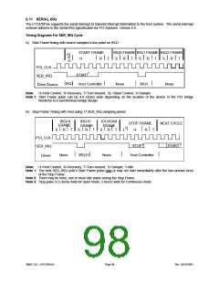
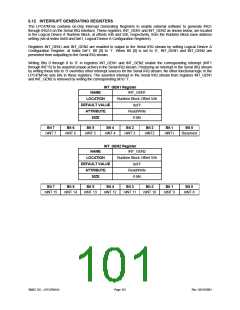
6.12 INTERRUPT GENERATING REGISTERS
The LPC47M14x contains on-chip Interrupt Generating Registers to enable external software to generate IRQ1
through IRQ15 on the Serial IRQ Interface. These registers, INT_GEN1 and INT_GEN2 as shown below, are located
in the Logical Device A Runtime Block, at offsets 54h and 55h, respectively, from the Runtime Block base address
setting (set at Index 0x60 and 0x61, Logical Device A Configuration Registers).
Registers INT_GEN1 and INT_GEN2 are enabled to output to the Serial IRQ stream by setting Logical Device A
Configuration Register, at Index 0xF1, Bit [0] to ‘1’. When Bit [0] is set to ‘0’, INT_GEN1 and INT_GEN2 are
prevented from outputting to the Serial IRQ stream.
Writing Bits 0 through 8 to ‘0’ in registers INT_GEN1 and INT_GEN2 enable the corresponding interrupt (INT1
through INT15) to be asserted (made active) in the Serial IRQ stream. Producing an interrupt in the Serial IRQ stream
by writing these bits to ‘0’ overrides other interrupt sources for the Serial IRQ stream. No other functional logic in the
LPC47M14x sets bits in these registers. The asserted interrupt in the Serial IRQ stream from registers INT_GEN1
and INT_GEN2 is removed by writing the corresponding bit to ‘1’.
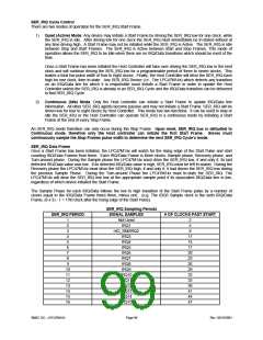
INT_GEN1 Register
NAME
LOCATION
DEFAULT VALUE
ATTRIBUTE
SIZE
INT_GEN1
Runtime Block Offset 54h
0xFF
Read/Write
8 bits
Bit 7
nINT 7
Bit 6
nINT 6
Bit 5
nINT 5
Bit 4
nINT 4
Bit 3
nINT 3
Bit 2
nINT2
Bit 1
nINT1
Bit 0
Reserved
INT_GEN2 Register
INT_GEN2
NAME
LOCATION
DEFAULT VALUE
ATTRIBUTE
SIZE
Runtime Block Offset 55h
0xFF
Read/Write
8 bits
Bit 7
nINT 15
Bit 6
nINT 14
Bit 5
nINT 13
Bit 4
nINT 12
Bit 3
nINT 11
Bit 2
nINT 10
Bit 1
nINT 9
Bit 0
nINT 8
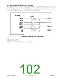
SMSC DS – LPC47M14X
Page 101
Rev. 03/19/2001

 SMSC [ SMSC CORPORATION ]