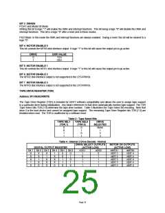
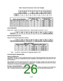
Table 5 - Internal 2 Drive Decode - Drives 0 and 1 Swapped
7
S/W
6
5
0
4
3
2
1
0
POWER
PRE-
PRE-
PRE-
DRATE DRATE
RESET DOWN
COMP2 COMP1 COMP0 SEL1
SEL0
RESET
COND.
0
0
0
0
0
0
1
0
DRIVE SELECT OUTPUTS
(ACTIVE LOW)
MOTOR ON OUTPUTS
(ACTIVE LOW)
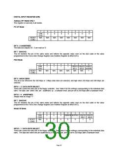
DIGITAL OUTPUT REGISTER
Bit 7 Bit 6 Bit 5 Bit 4 Bit1 Bit 0
nDS1
nDS0
nMTR1
nBIT 4
nBIT 4
nBIT 4
nBIT 4
nBIT 4
nMTR0
nBIT 5
nBIT 5
nBIT 5
nBIT 5
nBIT 5
X
X
X
1
X
X
1
X
0
X
1
X
X
0
1
X
X
X
0
0
0
1
1
X
0
1
0
1
X
0
1
1
1
1
1
0
1
1
1
0
Normal Floppy Mode
Normal mode. Register 3F3 contains only bits 0 and 1. When this register is read, bits 2 - 7 are ‘0’.
DB7
0
DB6
0
DB5
0
DB4
0
DB3
0
DB2
0
DB1
DB0
REG 3F3
tape sel1 tape sel0
Enhanced Floppy Mode 2 (OS2)
Register 3F3 for Enhanced Floppy Mode 2 operation.
DB7
DB6
DB5
DB4
DB3
DB2
DB1
DB0
REG 3F3 Reserved Reserved
Drive Type ID
Floppy Boot Drive
tape sel1 tape sel0
Table 6 - Drive Type ID
DIGITAL OUTPUT REGISTER REGISTER 3F3 - DRIVE TYPE ID
Bit 1
Bit 0
Bit 5
Bit 4
0
0
1
1
0
1
0
1
L0-CRF2 - B1
L0-CRF2 - B3
L0-CRF2 - B5
L0-CRF2 - B7
L0-CRF2 - B0
L0-CRF2 - B2
L0-CRF2 - B4
L0-CRF2 - B6
Note:
L0-CRF2-Bx = Logical Device 0, Configuration Register F2, Bit x.
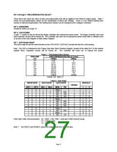
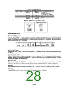
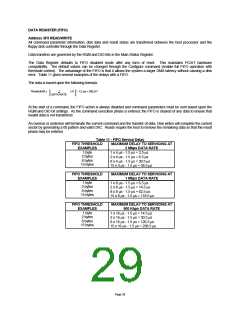
DATA RATE SELECT REGISTER (DSR)
Address 3F4 WRITE ONLY
This register is write only. It is used to program the data rate, amount of write precompensation, power down status, and
software reset. The data rate is programmed using the Configuration Control Register (CCR) not the DSR, for PC/AT
and PS/2 Model 30.
Other applications can set the data rate in the DSR. The data rate of the floppy controller is the most recent write of
either the DSR or CCR. The DSR is unaffected by a software reset. A hardware reset will set the DSR to 02H, which
corresponds to the default precompensation setting and 250 Kbps.
BIT 0 and 1 DATA RATE SELECT
These bits control the data rate of the floppy controller. See Table 8 for the settings corresponding to the individual data
rates. The data rate select bits are unaffected by a software reset, and are set to 250 Kbps after a hardware reset.
Page 26

 SMSC [ SMSC CORPORATION ]