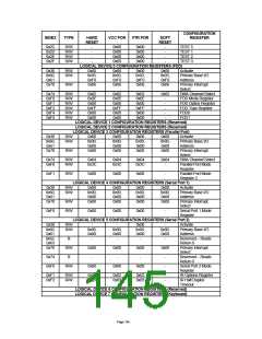
The following register is located at an offset of zero from (GAME_PORT) the address into the base I/O address
register for Logical Device 9.
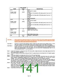
Table 61 - Game Port
REG OFFSET
NAME
(hex)
DESCRIPTION
Game Port Register
00
Game Port Register
Bit[0]
Bit[1]
Bit[2]
Bit[3]
Bit[4]
Bit[5]
Bit[6]
Bit[7]
X-Axis Joystick 1 (OUT1A)
Y-Axis Joystick 1 (OUT1B)
X-Axis Joystick 2 (OUT2A)
YAxis Joystick 2 (OUT2B)
Button Joystick 1 (J1B1)
Button Joystick 1 (J1B2)
Button Joystick 2 (J2B1)
Button Joystick 2 (J2B2)
Default = 0x00
on VTR POR
(R)
CONFIGURATION
The Configuration of the LPC47M10x is very flexible and is based on the configuration architecture implemented in
typical Plug-and-Play components. The LPC47M10x is designed for motherboard applications in which the resources
required by their components are known. With its flexible resource allocation architecture, the LPC47M10x allows the
BIOS to assign resources at POST.
SYSTEM ELEMENTS
Primary Configuration Address Decoder
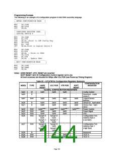
After a hard reset (nPCI_RESET pin asserted) or Vcc Power On Reset the LPC47M10x is in the Run Mode with all
logical devices disabled. The logical devices may be configured through two standard Configuration I/O Ports (INDEX
and DATA) by placing the LPC47M10x into Configuration Mode.
The BIOS uses these configuration ports to initialize the logical devices at POST. The INDEX and DATA ports are only
valid when the LPC47M10x is in Configuration Mode.
The SYSOPT pin is latched on the falling edge of the nPCI_RESET or on Vcc Power On Reset to determine the
configuration register's base address. The SYSOPT pin is used to select the CONFIG PORT's I/O address at power-up.
Once powered up the configuration port base address can be changed through configuration registers CR26 and CR27.
The SYSOPT pin is a hardware configuration pin which is shared with the GP24 signal on pin 45.
Note. An external pull-down resistor is required for the base IO address to be 0x02E for configuration. An external
pull-up resistor is required to move the base IO address for configuration to 0x04E.
The INDEX and DATA ports are effective only when the chip is in the Configuration State.
SYSOPT= 0
10k PULL-DOWN
RESISTOR
0x02E
SYSOPT= 1
10K PULL-UP
RESISTOR
0x04E
PORT NAME
CONFIG PORT (Note)
INDEX PORT (Note)
DATA PORT
TYPE
Write
Read/Write
Read/Write
0x02E
0x04E
INDEX PORT + 1
Note : The configuration port base address can be relocated through CR26 and CR27.
Page 142

 SMSC [ SMSC CORPORATION ]