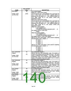
REG OFFSET
NAME
(hex)
DESCRIPTION
LED1
5D
LED1
Bit[1:0] LED1 Control
00=off
01=blink at 1Hz rate with a 50% duty cycle (0.5 sec on, 0.5
Default = 0x00
on VTR POR
(R/W)
sec off)
10=Blink at ½ HZ rate with a 25% duty cycle (0.5 sec on, 1.5
sec off)
11=on
Bits[7:2] Reserved
LED2
5E
LED2
Bit[1:0] LED2 Control
Default = 0x00
on VTR POR
(R/W)
00=off
01=blink at 1Hz rate with a 50% duty cycle (0.5 sec on, 0.5
sec off)
10=Blink at ½ HZ rate with a 25% duty cycle (0.5 sec on, 1.5
sec off)
11=on
Bits[7:2] Reserved
Keyboard Scan Code
Bit[0] LSB of Scan Code
. . .
Keyboard Scan
Code
5F
(R/W)
Default = 0x00
on VTR POR
. . .
. . .
Bit[7] MSB of Scan Code
N/A
60-7F
(R)
Reserved – reads return 0
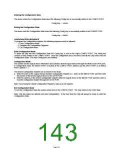
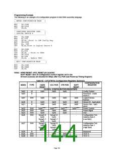
User Note:
When selecting an alternate function for a GPIO pin, all bits in the GPIO register must be properly
programmed, including in/out, polarity and output type. The polarity bit does not affect the DDRC
function or the either edge triggered interrupt functions.
User Note 1:
User Note 2:
If this pin is used for Ring Indicator wakeup, either the nRI2 event can be enabled via bit 1 in the
PME_EN1 register or the GP50 PME event can be enabled via bit 0 in the PME_EN5 register.
In order to use the P12, P16 and P17 functions, the corresponding GPIO must be programmed for
output, non-invert, and push-pull output type. The P17 function should not be selected on GP20
and GP 62 simultaneously. If P17 is selected on GP20 and GP62, simultaneously, then P17 on
GP62 will function and P17 on GP20 will not.
Note 1: If the EETI function is selected for this GPIO then both a high-to-low and a low-to-high edge will set the
PME, SMI and MSC status bits
Note 2: The IRTX2 function can be used on this pin if the IR Location Mux bit in the Serial Port 2 IR Option register
is set
Note 3: These pins default to an output and LOW on VCC POR and Hard Reset.
Note 4: If the FDC function is selected on this pin (nMTR1, nDS1, DRVDEN0, DRVDEN1) then bit 6 of the FDD
Mode Register (Configuration Register 0xF0 in Logical Device 0) will override bit 7 in the GPIO Control
Register. Bit 7 of the FDD Mode Register will also affect the pin if the FDC function is selected.
Note 5: The nIO_SMI pin is inactive when the internal group SMI signal is inactive and when the SMI enable bit
(EN_SMI, bit 7 of the SMI_EN2 register) is ‘0’. When the output buffer type is OD, nIO_SMI pin is floating
when inactive; when the output buffer type is push-pull, the nIO_SMI pin is high when inactive.
Note 6: Bits 2 and 3 of the PME_STS4 and SMI_STS4 registers, and bit 3 of the PME_STS5 register may be set on
a VCC POR. If GP32, GP33 and GP53 are configured as input, then their corresponding PME and SMI
status bits will be set on a VCC POR since these pins revert to their non-inverting GPIO output function
when VCC is removed from the part. These GPIOs cannot be used for PME wakeup when the part is under
VTR power (VCC=0).
Note 7: These bits are R/W but have no effect on circuit operation.
Page 141

 SMSC [ SMSC CORPORATION ]