Non-PCI Single-Chip Full Duplex Ethernet Controller
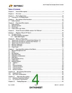
Table of Contents
Chapter 1 General Description .............................................................................................................6
Chapter 2 Overview ...............................................................................................................................7
Chapter 3 Pin Configurations .............................................................................................................10
3.1 Local Bus vs. Pin Requirements .......................................................................................................13
Chapter 4 Description of Pin Functions.............................................................................................15
4.1 Buffer Symbols..................................................................................................................................18
Chapter 5
Functional Description.......................................................................................................20
5.1 Buffer Memory...................................................................................................................................21
5.2 Interrupt Structure .............................................................................................................................27
5.3 Reset Logic........................................................................................................................................28
5.4 Power Down Logic States .................................................................................................................28
Chapter 6 Packet Format in Buffer memory for Ethernet...............................................................30
Chapter 7 Registers Map in I/O Space...............................................................................................33
7.1 I/O Space Access..............................................................................................................................34
7.2 I/O Space Registers Description.......................................................................................................35
7.2.1
Bank Select Register ..............................................................................................................................35
Chapter 8 Theory of Operation ..........................................................................................................59
8.1 Typical Flow Of Events For Transmit (Auto Release =0)..................................................................61
8.2 Typical Flow of Events for Transmit (Auto Release = 1)...................................................................62
8.3 Typical Flow Of Events For Receive.................................................................................................63
8.4 Memory Partitioning ..........................................................................................................................69
8.5 Interrupt Generation ..........................................................................................................................69
8.6 Power Down......................................................................................................................................71
Chapter 9 Functional Description of the Blocks................................................................................73
9.1 Memory Management Unit................................................................................................................73
9.2 Arbiter................................................................................................................................................73
9.3 Bus Interface .....................................................................................................................................74
9.4 Wait State Policy ...............................................................................................................................74
9.5 Arbitration Considerations.................................................................................................................75
9.6 DMA Block.........................................................................................................................................75
9.7 Packet Number FIFOs.......................................................................................................................76
9.8 CSMA Block ......................................................................................................................................77
9.9 Network Interface ..............................................................................................................................79
9.10
9.11
9.12
9.13
9.14
9.15
10BASE-T ......................................................................................................................................79
AUI .................................................................................................................................................79
Physical Interface...........................................................................................................................80
Transmit Functions.........................................................................................................................80
Transmit Drivers.............................................................................................................................80
Receive Functions..........................................................................................................................80
Chapter 10
Board Setup Information ...............................................................................................82
10.1
10.2
Diagnostic LEDs.............................................................................................................................83
Bus Clock Considerations..............................................................................................................83
Chapter 11
Operation Description ....................................................................................................85
11.1
11.2
Maximum Guaranteed Ratings*.....................................................................................................85
DC Electrical Characteristics .........................................................................................................86
Chapter 12
Timing Diagrams ............................................................................................................92
Rev. 11/18/2004
Page 4
SMSC DS – LAN91C96I
DATASHEET

 SMSC [ SMSC CORPORATION ]