Highly Efficient Single-Chip 10/100 Non-PCI Ethernet Controller
Datasheet
Chapter 6 Timing Diagrams
6.1
Host Interface Timing
The LAN9116 supports the following host cycles:
Read Cycles:
■
■
■
■
PIO Reads (nCS or nRD controlled)
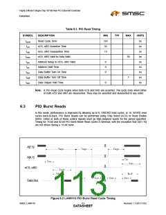
PIO Burst Reads (nCS or nRD controlled)
RX Data FIFO Direct PIO Reads (nCS or nRD controlled)
RX Data FIFO Direct PIO Burst Reads (nCS or nRD controlled)
Write Cycles:
■
PIO writes (nCS and nWR controlled)
TX Data FIFO direct PIO writes (nCS or nWR controlled)
■
6.1.1
Special Restrictions on Back-to-Back Write/Read Cycles
It is important to note that there are specific restrictions on the timing of back-to-back write-read
operations. These restrictions concern reading the control registers after any write cycle to the
LAN9116 device. In many cases there is a required minimum delay between writing to the LAN9116,
and the subsequent side effect (change in the control register value). For example, when writing to the
TX Data FIFO, it takes up to 135ns for the level indication to change in the TX_FIFO_INF register.
In order to prevent the host from reading stale data after a write operation, minimum wait periods must
be enforced. These periods are specified in Table 6.1, "Read After Write Timing Rules". The host
processor is required to wait the specified period of time after any write to the LAN9116 before reading
the resource specified in the table. These wait periods are for read operations that immediately follow
any write cycle. Note that the required wait period is dependant upon the register being read after the
write.
Performing "dummy" reads of the BYTE_TEST register is a convenient way to guarantee that the
minimum write-to-read timing restriction is met. Table 6.1 also shows the number of dummy reads that
are required before reading the register indicated. The number of BYTE_TEST reads in this table is
based on the minimum timing for Tcycle (165ns). For microprocessors with slower busses the number
of reads may be reduced as long as the total time is equal to, or greater than the time specified in the
table. Note that dummy reads of the BYTE_TEST register are not required as long as the minimum
time period is met.
Revision 1.1 (05-17-05)
110
SMSC LAN9116
DATASHEET

 SMSC [ SMSC CORPORATION ]