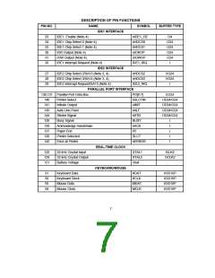
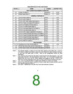
DESCRIPTION OF PIN FUNCTIONS
PIN NO.
NAME
SYMBOL
BUFFER TYPE
SOFT POWER MANAGEMENT INTERFACE
33
34
Power On (Note 4)
nPowerOn
I/O24
I/O24
Button Input (Note 4)
Button_In
GENERAL PURPOSE I/O
96
97
GP I/O; IRQ in (Note 4)
GP I/O; IRQ in (Note 4)
GP10
GP11
GP12
GP13
GP14
GP15
GP16
GP17
GP20
I/O4
I/O4
I/O4
I/O24
I/O4
I/O4
I/O4
I/O4
I/O4
I/O8
I/O8
I/O4
I/O4
I/O4
98
GP I/O; WD Timer Output /IRRX (Note 4)
GP I/O; Power Led output /IRTX (Note 4)
GP I/O; GP Address Decode (Note 4)
GP I/O; GP Write Strobe (Note 4)
99
100
102
103
104
105
106
107
108
109
110
GP I/O; Joy Read Strobe/JOYCS (Note 4)
GP I/O; Joy Write Strobe (Note 4)
GP I/O; IDE2 Output Enable/8042 P20 (Note 4)
GP I/O; Serial EEPROM Data In/AB_DATA (Note 4) GP21
GP I/O; Serial EEPROM Data Out/AB_CLK (Note 4) GP22
GP I/O; Serial EEPROM Clock (Note 4)
GP I/O; Serial EEPROM Enable (Note 4)
GP I/O; 8042 P21 (Note 4)
GP23
GP24
GP25
BIOS BUFFERS
111:118 ROM Bus (I/O to the SD Bus) (Note 4)
RD[0:7]
I/O4
119
120
ROM Chip Select (only used for ROM) (Note 4)
nROMCS
I
I
ROM Output Enable (DIR) (only used for ROM) (Note 4) nROMDIR
Note 0:
The interrupt request is output on one of the IRQx signals as 024 buffer type. If EPP or
ECP Mode is enabled, this output is pulsed low, then released to allow sharing of interrupts.
In this case, the buffer type is OD24. Refer to the configuration section for more
information.
Note 1:
nCS -This pin is the active low chip select; it must be low for all chip accesses. For 12 bit
addressing, SA0:SA11, this input should be tied to GND. For 16 bit address qualification,
address bits SA12:SA15 can be "ORed" together and applied to this pin. If IDE2 is not
used, SA12 can be connected to nCS, pin 27 to SA13, pin 28 to SA14 and pin 29 to SA15
nYY - The "n" as the first letter of a signal name indicates an "Active Low" signal
nHDCS2 and nHDCS3 require a pull-up to ensure a logic high at power-up when used for
IDE2 until the Active Bit is set to 1.
Note 2:
Note 3:
Note 4:
See Table 1, Multifunction Pins with GPI/O and Other Alternate Functions.
8

 SMSC [ SMSC CORPORATION ]