with standard ISA devices. The port is equivalent to a generic parallel port interface and may be operated in that
mode. The port registers vary depending on the mode field in the ecr (Table 68). Table 67 lists these dependencies.
Operation of the devices in modes other that those specified is undefined.
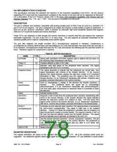
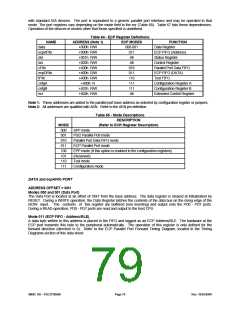
Table 64 - ECP Register Definitions
NAME
ADDRESS (Note 1)
+000h R/W
+000h R/W
+001h R/W
+002h R/W
+400h R/W
+400h R/W
+400h R/W
+400h R
ECP MODES
FUNCTION
Data Register
ECP FIFO (Address)
Status Register
data
000-001
011
All
ecpAFifo
dsr
dcr
All
Control Register
cFifo
ecpDFifo
tFifo
cnfgA
cnfgB
ecr
010
011
110
111
111
All
Parallel Port Data FIFO
ECP FIFO (DATA)
Test FIFO
Configuration Register A
Configuration Register B
Extended Control Register
+401h R/W
+402h R/W
Note 1: These addresses are added to the parallel port base address as selected by configuration register or jumpers.
Note 2: All addresses are qualified with AEN. Refer to the AEN pin definition.
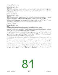
Table 65 - Mode Descriptions
DESCRIPTION
MODE
000
001
010
011
100
101
110
111
(Refer to ECR Register Description)
SPP mode
PS/2 Parallel Port mode
Parallel Port Data FIFO mode
ECP Parallel Port mode
EPP mode (If this option is enabled in the configuration registers)
(Reserved)
Test mode
Configuration mode
DATA and ecpAFifo PORT
ADDRESS OFFSET = 00H
Modes 000 and 001 (Data Port)
The Data Port is located at an offset of ‘00H’ from the base address. The data register is cleared at initialization by
RESET. During a WRITE operation, the Data Register latches the contents of the data bus on the rising edge of the
nIOW input. The contents of this register are buffered (non inverting) and output onto the PD0 - PD7 ports.
During a READ operation, PD0 - PD7 ports are read and output to the host CPU.
Mode 011 (ECP FIFO - Address/RLE)
A data byte written to this address is placed in the FIFO and tagged as an ECP Address/RLE. The hardware at the
ECP port transmits this byte to the peripheral automatically. The operation of this register is only defined for the
forward direction (direction is 0). Refer to the ECP Parallel Port Forward Timing Diagram, located in the Timing
Diagrams section of this data sheet.
SMSC DS – FDC37N3869
Page 79
Rev. 10/25/2000

 SMSC [ SMSC CORPORATION ]