cnfgA (Configuration Register A)
ADDRESS OFFSET = 400H
Mode = 111
This register is a read only register. When read, 10H is returned. This indicates to the system that this is an 8-bit
implementation. (PWord = 1 byte)
cnfgB (Configuration Register B)
ADDRESS OFFSET = 401H
Mode = 111
BIT 7 compress
This bit is read only. During a read it is a low level. This means that this chip does not support hardware RLE
compression. It does support hardware de-compression!
BIT 6 intrValue
Returns the value on the ISA iRq line to determine possible conflicts.
BITS 5:0 Reserved
During a read are a low level. These bits cannot be written.
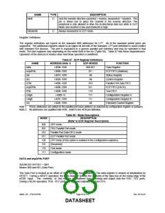
ecr (Extended Control Register)
ADDRESS OFFSET = 402H
Mode = all
This register controls the extended ECP parallel port functions (Table 69).
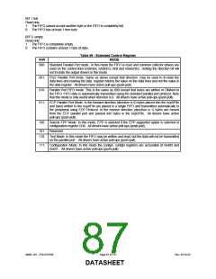
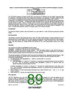
BITS 7,6,5
These bits are Read/Write and select the Mode.
BIT 4 nErrIntrEn
Read/Write (Valid only in ECP Mode)
1: Disables the interrupt generated on the asserting edge of nFault.
0: Enables an interrupt pulse on the high to low edge of nFault. Note that an interrupt will be generated if nFault is
asserted (interrupting) and this bit is written from a “1” to a “0”. This prevents interrupts from being lost in the time
between the read of the ecr and the write of the ecr.
BIT 3 dmaEn
Read/Write
1: Enables DMA (DMA starts when serviceIntr is “0”).
0: Disables DMA unconditionally.
BIT 2 serviceIntr
Read/Write
1: Disables DMA and all of the service interrupts.
0: Enables one of the following 3 cases of interrupts. Once one of the 3 service interrupts has occurred serviceIntr bit
shall be set to a “1” by hardware, it must be reset to “0” to re-enable the interrupts. Writing this bit to a “1” will not
cause an interrupt.
case dmaEn=1:
During DMA (this bit is set to a “1” when terminal count is reached).
case dmaEn=0 direction=0:
This bit shall be set to “1” whenever there are writeIntrThreshold or more bytes free in the FIFO.
case dmaEn=0 direction=1:
This bit shall be set to “1” whenever there are readIntrThreshold or more valid bytes to be read from the FIFO.
SMSC DS – FDC37N769
Page 86 of 137
Rev. 02-16-07
DATASHEET

 SMSC [ SMSC CORPORATION ]