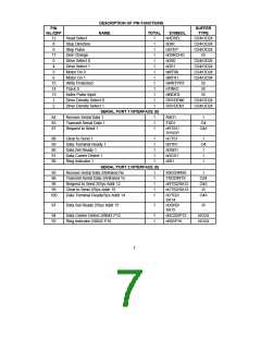
FUNCTIONAL DESCRIPTION
SUPER I/O REGISTERS
HOST PROCESSOR INTERFACE
The address map, shown below in Table 1,
shows the addresses of the different blocks of
the Super I/O immediately after power up. The
base addresses of the FDC, serial and parallel
ports can be moved via the configuration
registers. Some addresses are used to access
more than one register.
The host processor communicates with the
FDC37M60x through a series of read/write
registers. The port addresses for these registers
are shown in Table 1. Register access is
accomplished through programmed I/O or DMA
transfers. All registers are 8 bits wide. All host
interface output buffers are capable of sinking a
minimum of 24 mA.
Table 1 - Super I/O Block Addresses
LOGICAL
DEVICE
ADDRESS
Base+(0-5) and +(7)
Base+(0-7)
BLOCK NAME
NOTES
Floppy Disk
0
4
5
3
Serial Port Com 1
Serial Port Com 2
Base1+(0-7)
IR Support
Parallel Port
SPP
Base+(0-3)
Base+(0-7)
EPP
Base+(0-3), +(400-402)
Base+(0-7), +(400-402)
ECP
ECP+EPP+SPP
60, 64
KYBD
7
Note 1: Refer to the configuration register descriptions for setting the base address
11

 SMSC [ SMSC CORPORATION ]