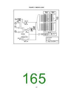
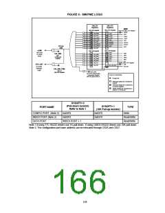
FIGURE 6 - SMI/PME LOGIC
SMI_EN
Registers
SMI_STS
Registers
EVENT
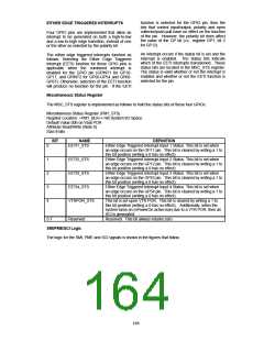
SMI_STS1 Register
SMI_EN1 Register
RING Bit, PME_STS1 Register
nRING
EN_RING
PINT
PINT
configuration ports to initialize the logical devices
EN_PINT
CONFIGURATION
U2INT
U2INT
EN_U2INT
U1INT
at POST. The INDEX and DATA ports are only
U1INT
EN_U1INT
FINT
FINT
valid when the FDC37B78x is in Configuration
The Configuration of the FDC37B78x is very
flexible and is based on the configuration
EN_FINT
GPINT2
GPINT1
WDT
GPINT2
GPINT1
WDT
Mode.
EN_GPINT2
EN_GPINT1
EN_WDT
Group
architecture implemented in typical Plug-and-Play
componneSnMtsI . The FDC37B78x is designed for
SMI
The SYSOPT pin is latched on the falling edge of
SMI_STS2 Register
SMI_EN2 Register
the RESET_DRV or on Vcc Power On Reset to
out to pin
motherboard applicationEsN_inSMwI hich the resources
MINT
KINT
MINT
or Serial
EN_MINT
determine the configuration register's base
required by their components are known. With its
KINT
IRINT
Bit 7
of SMI_EN2
flexible IRrQe2source allocRaetgiiostenr architecture, the
EN_KINT
IRINT
address. The SYSOPT pin is used to select the
EN_IRINT
BINT
CONFIG PORT's I/O address at BpINoTwer-up. Once
EN_BINT
P12
FDC37B78x allows the BIOS to assign resources
P12
EN_P12
CIR Bit, PME_STS1 Register
powered up the configuration port base address
at POST.
DEV_INT
CIR
EN_CIR
SLP_EN_SMI
can be changed through configuration registers
SLP_EN
to nPME
Interface
SYSTEM ELEMENTS EN_SMI_PME
CR26 and CR27. The SYSOPT pin is a
Logic
Bit 6 of
ha
S
r
L
dwa
RLre configuration pin which is shared
P_
CT
SMI_EN2 Register
Biwt 0 oiftthhe StlehepeEnanbleRTS1 sigKneayltooSnympbionls 115. During reset
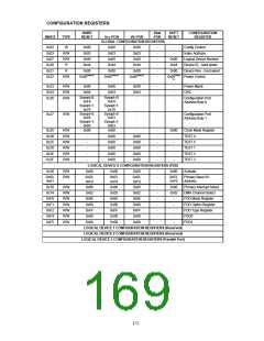
Primary Configuration Address Decoder
Configuration Register
0xtFh0 oisf Logpicainl Deviisce Aa. weak actiEvneablleobwit signal which sinks
30µA. Note: All I/O addresses are qualified with
After a hard reset (RESET_DRV pin asserted) or
Vcc Power On Reset the FDC37B78x is in the
Run Mode with all logical devices disabled. The
logical devices may be configured through two
standard Configuration I/O Ports (INDEX and
Interrupt Status bit: Cleared at
source
AEN.
Interrupt Status bit: Cleared by
a read of register
Sticky Status bit: Cleared by a
The INDEX and DATA ports are effective only
write of ‘1’ to this bit
when the chip is in the Configuration State.
DATA)
by
placing
the FDC37B78x into
Configuration Mode.
The BIOS uses these
SYSOPT= 0
(Pull-down resistor)
Refer to Note 1
SYSOPT= 1
(10K Pull-up resistor)
PORT NAME
TYPE
Write
CONFIG PORT (Note 2)
INDEX PORT (Note 2)
DATA PORT
0x03F0
0x0370
0x0370
0x03F0
Read/Write
Read/Write
INDEX PORT + 1
Note 1:If using TTL RS232 drivers use 1K pull-down. If using CMOS RS232 drivers use 10K pull-down.
Note 2: The configuration port base address can be relocated through CR26 and CR27.
168

 SMSC [ SMSC CORPORATION ]