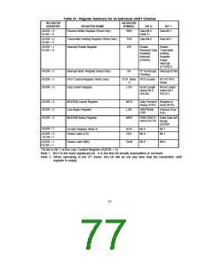
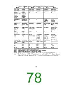
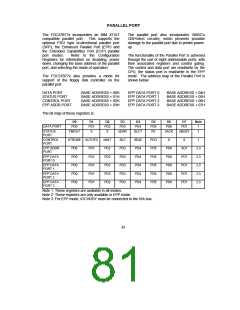
Table 33 - Register Summary for an Individual UART Channel
REGISTER
REGISTER
ADDRESS*
REGISTER NAME
SYMBOL
BIT 0
BIT 1
ADDR = 0
DLAB = 0
Receive Buffer Register (Read Only)
RBR
Data Bit 0
(Note 1)
Data Bit 1
ADDR = 0
DLAB = 0
Transmitter Holding Register (Write Only)
Interrupt Enable Register
THR
IER
Data Bit 0
Data Bit 1
Enable
ADDR = 1
DLAB = 0
Enable
Received Data Transmitter
Available
Interrupt
(ERDAI)
Holding
Register
Empty
Interrupt
(ETHREI)
ADDR = 2
ADDR = 2
ADDR = 3
Interrupt Ident. Register (Read Only)
FIFO Control Register (Write Only)
Line Control Register
IIR
"0" if Interrupt Interrupt ID Bit
Pending
FCR (Note FIFO Enable
7)
RCVR FIFO
Reset
LCR
Word Length
Select Bit 0
(WLS0)
Word Length
Select Bit 1
(WLS1)
ADDR = 4
ADDR = 5
ADDR = 6
MODEM Control Register
Line Status Register
MCR
LSR
Data Terminal Request to
Ready (DTR) Send (RTS)
Data Ready
(DR)
Overrun Error
(OE)
Delta Clear to
Send (DCTS)
MODEM Status Register
MSR
Delta Data Set
Ready
(DDSR)
ADDR = 7
Scratch Register (Note 4)
Divisor Latch (LS)
SCR
DDL
Bit 0
Bit 0
Bit 1
Bit 1
ADDR = 0
DLAB = 1
ADDR = 1
DLAB = 1
Divisor Latch (MS)
DLM
Bit 8
Bit 9
*DLAB is Bit 7 of the Line Control Register (ADDR = 3).
Note 1: Bit 0 is the least significant bit. It is the first bit serially transmitted or received.
Note 2: When operating in the XT mode, this bit will be set any time that the transmitter shift
register is empty.
77

 SMSC [ SMSC CORPORATION ]