GP INDEX REGISTERS
The Watchdog Timer Control, SMI Enable and
To access these registers when in normal (run)
mode, the host should perform an IOW of the
Register Index to the GP Index register (at
0xEX) to select the Register and then read or
write the Data register (at Index+1) to access
the register.
SMI Status Registers can be accessed by the
host when the chip is in the normal run mode if
CR03 Bit[7]=1. The host uses GP Index and
Data register to access these registers. The
Power on default GP Index and Data registers
are 0xEA and 0xEB respectively. In
configuration mode the GP Index address may
be programmed to reside on addresses 0xE0,
0xE2, 0xE4 or 0xEA. The GP Data address is
automatically set to the Index address + 1. Upon
exiting the configuration mode the new GP Index
and Data registers are used to access registers
WDT_CTRL, SMI Enable and SMI Status
Registers.
The WDT_CTRL, SMI Enable and SMI Status
registers can also be accessed by the host when
in the configuration state through Logical Device
8.
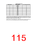
Table 47A - GP Index and Data Register
REGISTER
GP Index
GP Data
ADDRESS (R/W)
NORMAL (RUN) MODE
0xE0, E2, E4, EA
Index address + 1
0x01-0x0F
Access to Watchdog Timer
Control, SMI Enable and
SMI Status Registers (see
Table 47B)
117

 SMSC [ SMSC CORPORATION ]