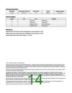
DATA SHEET • CX77107
PA MODULE FOR CDMA / PCS (1850–1910 MHZ)
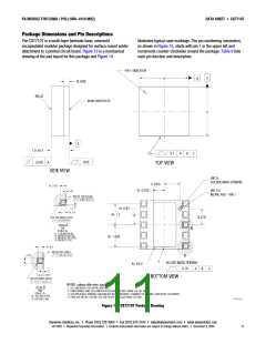
Package and Handling Information
Because of its sensitivity to moisture absorption, this device
package is baked and vacuum-packed prior to shipment.
Instructions on the shipping container label must be followed
regarding exposure to moisture after the container seal is broken,
otherwise, problems related to moisture absorption may occur
when the part is subjected to high temperature during solder
assembly.
The CX77107 is capable of withstanding an MSL 3/240 °C solder
reflow. Care must be taken when attaching this product, whether
it is done manually or in a production solder reflow environment.
If the part is attached in a reflow oven, the temperature ramp rate
should not exceed 5 °C per second; maximum temperature
should not exceed 240 °C. If the part is manually attached,
precaution should be taken to insure that the part is not subjected
to temperatures exceeding 240 °C for more than 10 seconds. For
details on both attachment techniques, precautions, and handling
procedures recommended by Skyworks, please refer to Skyworks
Application Note: PCB Design and SMT Assembly/Rework,
Document Number 101752. Additional information on standard
SMT reflow profiles can also be found in the JEDEC Standard J–
STD–020B.
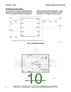
Figure 14 Typical Case Markings (Top View)
Production quantities of this product are shipped in the standard
tape-and-reel format. For packaging details, refer to Skyworks
Application Note: Tape and Reel Information–RF Modules,
Document Number 101568.
Electrostatic Discharge Sensitivity
The CX77107 is a Class I device. lists the Electrostatic Discharge
(ESD) immunity level for each pin of the CX77107 product. The
numbers in specify the ESD threshold level for each non-ground
pin where the I-V curve between the pin and ground starts to
show degradation.
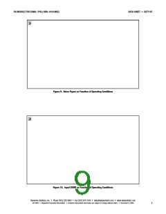
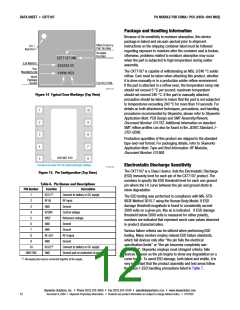
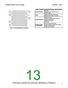
Figure 15. Pin Configuration (Top View)
Table 6. Pin Names and Descriptions
PIN Number
Function
VCC1 (1)
RF IN
Description
Connect to battery or DC supply
RF Input
1
The ESD testing was performed in compliance with MIL-STD-
883E Method 3015.7 using the Human Body Model. If ESD
damage threshold magnitude is found to consistently exceed
2000 volts on a given pin, this so is indicated. If ESD damage
threshold below 2000 volts is measured for either polarity,
numbers are indicated that represent worst case values observed
in product characterization.
2
3
GND
Ground
4
VCONT
VREF
Control voltage
5
Reference voltage
Ground
6
GND
7
GND
Ground
Various failure criteria can be utilized when performing ESD
testing. Many vendors employ relaxed ESD failure standards,
which fail devices only after “the pin fails the electrical
specification limits” or “the pin becomes completely non-
functional”. Skyworks employs most stringent criteria; fails
devices as soon as the pin begins to show any degradation on a
curve tracer. To avoid ESD damage, both latent and visible, it is
very important that the product assembly and test areas follow
the Class-1 ESD handling precautions listed in Table 7.
8
RF OUT
GND
RF Output
9
10
Ground
VCC2 (1)
Connect to battery or DC supply
Ground pad on underside of package
GND PAD
GND
(1)
All supply pins may be connected together at the supply.
Skyworks Solutions, Inc. • Phone [781] 376-3000 • Fax [781] 376-3100 • sales@skyworksinc.com • www.skyworksinc.com
December 8, 2004 • Skyworks Proprietary Information. • Products and product information are subject to change without notice. • 101782D
12

 SKYWORKS [ SKYWORKS SOLUTIONS INC. ]