ST7735
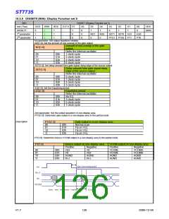
10.2.5 DISSET5 (B6h): Display Function set 5
B6H
DISSET (Display Function set 5)
Inst / Para
D/CX
WRX
RDX
D17-8 D7
D6
0
D5
1
D4
1
D3
D2
1
D1
1
D0
HEX
DISSET5
0
1
1
↑
↑
↑
1
1
1
-
-
-
1
0
0
0
0
(B6h)
1st parameter
2nd parameter
0
NO1
0
NO0
0
SDT1
SDT0 EQ1
EQ0
PT0
0
PTG1 PTG0 PT1
1st parameter: Set output waveform relation.
-NO[1:0]: Set the amount of non-overlap of the gate output
Amount of non-overlap of the gate
output
NO[1:0]
Refer the Internal oscillator
1 clock cycle
2 clock cycle
4 clock cycle
6 clock cycle
00
01
10
11
00h
01h
02h
03h
-SDT[1:0]: Set delay amount from gate signal rising edge of the source output
.
Delay amount form gate signal rising
edge of the source output
SDT[1:0]
Refer the Internal oscillator
00
01
10
11
00h
01h
02h
03h
0 clock cycle
1 clock cycle
2 clock cycle
3 clock cycle
-EQ[1:0]: Set the Equalizing period
EQ[1:0]
Equalizing period
Refer the Internal oscillator
No EQ
3 clock cycle
5 clock cycle
7 clock cycle
00
01
10
11
00h
01h
02h
03h
-2nd parameter: Set the output waveform in non-display area.
-PTG[1:0]: Determine gate output in a non-display area in the partial mode
Description
PTG[1:0]
Gate output in a non-display area
Normal scan
Fix on VGL
Fix on VGL
Fix on VGL
00
01
10
11
00h
01h
02h
03h
-PT[1:0]: Determine Source /VCOM output in a non-display area in the partial mode
PT[1:0]
Source output on non-display area
VCOM output on non-display area
Positive
V63
V0
AGND
Hi-z
Negative
V0
V63
AGND
Hi-z
Positive
VCOML
VCOML
AGND
Negative
VCOMH
VCOMH
AGND
00
01
10
11
00h
01h
02h
03h
AGND
AGND
V1.7
126
2009-12-04

 SITRONIX [ SITRONIX TECHNOLOGY CO., LTD. ]