ABSOLUTE MAXIMUM RATINGS
These are stress ratings only and functional operation of the device at
theseratingsoranyotherabovethoseindicatedintheoperationsections
ofthespecificationsbelowisnotimplied. Exposuretoabsolutemaximum
rating conditions for extended periods of time may affect reliability.
VCC............................................................................................................+7V
Input Voltages
Output Voltages
Logic........................................................-0.3Vto(VCC+0.5V)
Drivers...................................................................... ±15V
Receivers............................................-0.3V to (VCC+0.5V)
StorageTemperature.......................................................-65˚Cto+150˚C
Power Dissipation per Package
8-pin NSOIC (derate 6.60mW/oC above +70oC)...........................550mW
8-pin PDIP (derate 11.8mW/oC above +70oC)............................1000mW
Logic........................................................-0.3Vto(VCC+0.5V)
Drivers..................................................-0.3Vto(VCC+0.5V)
Receivers................................................................. ±15V
SPECIFICATIONS
TMIN to TMAX and VCC = 5V ± 5% unless otherwise noted.
PARAMETERS
MIN.
TYP.
MAX. UNITS CONDITIONS
SP481E/SP485E DRIVER
DC Characteristics
Differential Output Voltage
GND
2
VCC
VCC
Volts
Volts
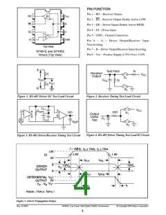
Unloaded; R = ∞ ; see Figure 1
with load; R = 50Ω; (RS-422);
see Figure 1
Differential Output Voltage
Differential Output Voltage
Change in Magnitude of Driver
Differential Output Voltage for
Complimentary States
Driver Common-Mode
Output Voltage
Input High Voltage
Input Low Voltage
Input Current
1.5
VCC
Volts
Volts
with load; R = 27Ω; (RS-485);see Figure 1
0.2
3
R = 27Ω or R = 50Ω; see Figure 1
Volts
Volts
Volts
µA
R = 27Ω or R = 50Ω; see Figure 1
Applies to DE, DI, RE
Applies to DE, DI, RE
2.0
0.8
±10
Applies to DE, DI, RE
Driver Short-Circuit Current
VOUT = HIGH
VOUT = LOW
±250 mA
±250 mA
-7V ≤ VO ≤ +12V
-7V ≤ VO ≤ +12V
SP481E/SP485E DRIVER
AC Characteristics
Maximum Data Rate
10
20
20
Mbps
ns
RE = 5V, DE = 5V; RDIFF = 54Ω,
CL1 = CL2 = 100pF
tPLH; RDIFF = 54Ω, CL1 = CL2 = 100pF;
see Figures 3 and 5
tPLH; RDIFF = 54Ω, CLI = CL2 = 100pF;
See Figures 3 and 5
Driver Input to Output
30
30
60
80
Driver Input to Output
(SP485EMN ONLY)
ns
Driver Input to Output
20
20
30
30
5
60
80
10
40
70
70
70
70
ns
ns
ns
ns
ns
ns
ns
ns
tPHL; RDIFF = 54Ω, CL1 = CL2 = 100pF;
see Figures 3 and 5
tPHL; RDIFF = 54Ω, CL1 = CL2 = 100pF;
see Figures 3 and 5
Driver Input to Output
(SP485EMN ONLY)
Driver Skew
see Figures 3 and 5,
tSKEW = | tDPLH - tDPHL
|
Driver Rise or Fall Time
3
15
40
40
40
40
From 10% to 90%; RDIFF = 54Ω,
CL1 = CL2 = 100pF; see Figures 3 &
CL = 100pF; see Figures 4 & 6; S2
6
Driver Enable to Output High
closed
Driver Enable to Output Low
closed
Driver Disable Time from Low
closed
Driver Disable Time from High
closed
CL = 100pF; see Figures 4 & 6; S1
CL = 100pF; see Figures 4 & 6; S1
CL = 100pF; see Figures 4 & 6; S2
Rev. 5/16/03
SP481E Low Power Half-Duplex RS485 Transceivers
© Copyright 2003 Sipex Corporation
2

 SIPEX [ SIPEX CORPORATION ]