The charge pump operates in a discontinuous
mode using an internal oscillator. If the output
voltages are less than a magnitude of 5.5V, the
charge pump is enabled. If the output voltages
exceed a magnitude of 5.5V, the charge pump is
disabled. Thisoscillatorcontrolsthefourphases
of the voltage shifting. A description of each
phase follows.
®
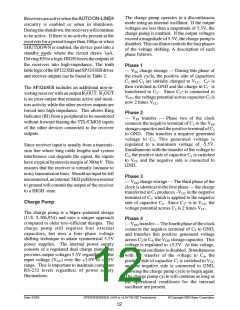
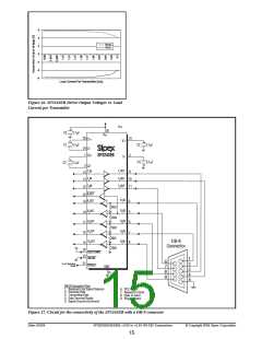
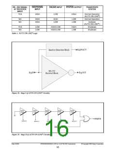
ReceiversareactivewhentheAUTOON-LINE
circuitry is enabled or when in shutdown.
Duringtheshutdown, thereceiverswillcontinue
to be active. If there is no activity present at the
receivers for a period longer than 100µs or when
SHUTDOWN is enabled, the device goes into a
standby mode where the circuit draws 1µA.
DrivingENtoalogicHIGHforcestheoutputsof
the receivers into high-impedance. The truth
tablelogicoftheSP3223EBandSP3243EBdriver
and receiver outputs can be found in Table 2.
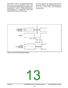
Phase 1
— VSS charge storage — During this phase of
the clock cycle, the positive side of capacitors
+
C1 and C2 are initially charged to VCC. Cl is
–
then switched to GND and the charge in C1 is
The SP3243EB includes an additional non-in-
verting receiver with an output R2OUT. R2OUT
is an extra output that remains active and moni-
tors activity while the other receiver outputs are
forced into high impedance. This allows Ring
Indicator (RI) from a peripheral to be monitored
without forward biasing the TTL/CMOS inputs
of the other devices connected to the receiver
outputs.
–
+
transferred to C2 . Since C2 is connected to
VCC, the voltage potential across capacitor C2 is
now 2 times VCC
.
Phase 2
— VSS transfer — Phase two of the clock
connects the negative terminal of C2 to the VSS
storage capacitor and the positive terminal of C2
to GND. This transfers a negative generated
voltage to C3. This generated voltage is
regulated to a minimum voltage of -5.5V.
Simultaneous with the transfer of the voltage to
C3, the positive side of capacitor C1 is switched
to VCC and the negative side is connected to
GND.
Since receiver input is usually from a transmis-
sion line where long cable lengths and system
interference can degrade the signal, the inputs
haveatypicalhysteresismarginof300mV. This
ensures that the receiver is virtually immune to
noisy transmission lines. Should an input be left
unconnected, aninternal 5KΩpulldownresistor
to ground will commit the output of the receiver
to a HIGH state.
Phase 3
— VDD charge storage — The third phase of the
clock is identical to the first phase — the charge
transferred in C1 produces –VCC in the negative
terminal of C1, which is applied to the negative
Charge Pump
+
side of capacitor C2. Since C2 is at VCC, the
voltage potential across C2 is 2 times VCC
.
The charge pump is a Sipex–patented design
(U.S. 5,306,954) and uses a unique approach
compared to older less–efficient designs. The
charge pump still requires four external
capacitors, but uses a four–phase voltage
shifting technique to attain symmetrical 5.5V
power supplies. The internal power supply
consists of a regulated dual charge pump that
provides output voltages 5.5V regardless of the
input voltage (VCC) over the +3.0V to +5.5V
range. This is important to maintain compliant
RS-232 levels regardless of power supply
fluctuations.
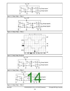
Phase 4
— VDD transfer — The fourth phase of the clock
connects the negative terminal of C2 to GND,
and transfers this positive generated voltage
across C2 to C4, the VDD storage capacitor. This
voltage is regulated to +5.5V. At this voltage,
the internal oscillator is disabled. Simultaneous
with the transfer of the voltage to C4, the
positive side of capacitor C1 is switched to VCC
and the negative side is connected to GND,
allowing the charge pump cycle to begin again.
The charge pump cycle will continue as long as
the operational conditions for the internal
oscillator are present.
Date: 6/2/04
SP3223EB/3243EB +3.0V to +5.5V RS-232 Transceivers
© Copyright 2004 Sipex Corporation
12

 SIPEX [ SIPEX CORPORATION ]