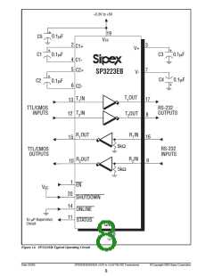
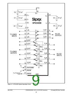
+3V to +5V
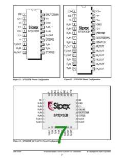
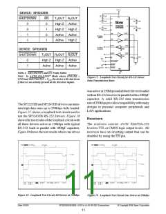
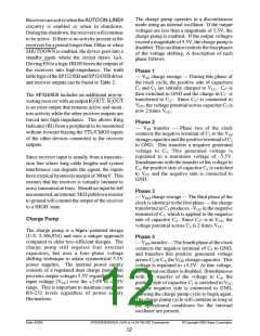
DEVICE: SP3223EB
+
0.1µF
0.1µF
C5
C1
VCC
SHUTDOWN
EN
0
TXOUT RXOUT
High Z Active
High Z High Z
C1+
V+
V-
+
+
+
C3
C4
0.1µF
0.1µF
C1-
0
0
1
1
C2+
SP3223EB
SP3243EB
+
C2
0.1µF
1
C2-
T1OUT
T1IN
0
Active
Active
Active
High Z
TTL/CMOS
INPUTS
TXIN
TXOUT
1
R1OUT
R1IN
TTL/CMOS
OUTPUTS
5kΩ
DEVICE: SP3243EB
R
XOUT
RXIN
SHUTDOWN
TXOUT RXOUT R2OUT
5kΩ
1000pF
1000pF
EN
VCC
0
1
High Z High Z
Active Active
Active
Active
SHUTDOWN
ONLINE
STATUS
To µP Supervisor
Circuit
GND
18
Table 2. SHUTDOWN and EN Truth Tables
Note: In AUTO ON-LINE® Mode where ONLINE =
GND and SHUTDOWN = VCC, the device will shut down
if there is no activity present at the Receiver inputs.
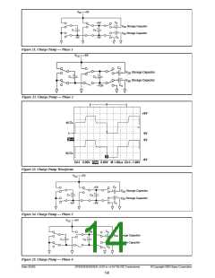
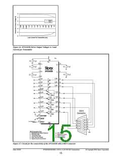
Figure 17. Loopback Test Circuit for RS-232 Driver
Data Transmission Rates
wasactiveat250kbpsandallthreedriversloaded
withanRS-232receiverinparallelwitha1000pF
capacitor. A solid RS-232 data transmission
rateof250kbpsprovidescompatibilitywithmany
designs in personal computer peripherals and
LAN applications.
TheSP3223EBandSP3243EBdriverscanmain-
tain high data rates up to 250kbps fully loaded.
Figure 17. shows a loopback test circuit used to
test the SP3243EB RS-232 Drivers. Figure 18
showsthetestresultsoftheloopbackcircuitwith
all three drivers active at 120kbps with typical
RS-232 loads in parallel with 1000pF capacitors.
Figure19 shows the test results where one driver
Receivers
The receivers convert ±5.0V EIA/TIA-232
levels to TTL or CMOS logic output levels. All
receivers have an inverting output that can be
disabled by using the EN pin.
Figure 18. Loopback Test Circuit All Drivers at 120kbps
Figure 19. Loopback Test Circuit One Driver at 250kbps
Date: 6/2/04
SP3223EB/3243EB +3.0V to +5.5V RS-232 Transceivers
© Copyright 2004 Sipex Corporation
11

 SIPEX [ SIPEX CORPORATION ]