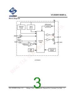
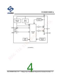
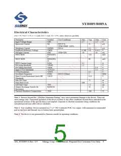
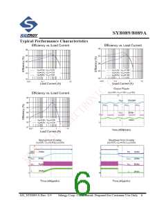
SY8089/8089A
VOUT
R1
Operation Principle
SY8089 is a synchronous buck regulator IC that
integrates the PWM control, top and bottom switches
on the same die to minimize the switching transition
loss and conduction loss. With ultra low RDS(ON) power
switches and proprietary PWM control, this regulator
IC can achieve the highest efficiency and the highest
switch frequency simultaneously to minimize the
external inductor and capacitor size, and thus achieving
the minimum solution footprint.
FB
R2
GND
Input capacitor CIN:
This ripple current through input capacitor is calculated
as:
ICIN_RMS =IOUT × D(1-D)
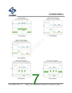
Short Circuit Protection
This formula has a maximum at VIN=2VOUT condition,
where ICIN_RMS=IOUT/2. This simple worst-case
condition is commonly used for DC/DC design.
(SY8089)After the soft start is over, if the output
voltage falls below 40% of the regulation level, IC will
turn off both power switches, entering short circuit
protection. It will remain in this state until the IN or EN
voltage is recycled.
With the maximum load current at 2.0A. A typical
X5R or better grade ceramic capacitor with 6.3V rating
and more than 1 pcs 22µF capacitor can handle this
ripple current well. To minimize the potential noise
problem, ceramic capacitor should really be placed
close to the IN and GND pins. Care should be taken to
minimize the loop area formed by CIN, and IN/GND
pins
(SY8089A) The frequency is folded back to about 30%
of the nominal frequency and the current limit is folded
back to 3.0A to prevent the inductor current from
runaway and to reduce the power dissipation of the IC
under short circuit conditions.
Over-voltage Protection
If the output voltage exceeds 120% of the regulation
level for more than 20µs, IC will turn off both power
switches and turn on the discharge switch, entering
over-voltage protection. It will remain in this state until
IN or EN voltage is recycled.
Output capacitor COUT:
The output capacitor is selected to handle the output
ripple noise requirements. Both steady state ripple and
transient requirements must be taken into consideration
when selecting this capacitor. For the best performance,
it is recommended to use X5R or better grade ceramic
capacitor with 6.3V rating and greater than 22µF
capacitance.
Applications Information
Because of the high integration in the SY8089 IC, the
application circuit based on this regulator IC is rather
simple. Only input capacitor CIN, output capacitor COUT
output inductor L and feedback resistors (R1 and R2)
need to be selected for the targeted applications
specifications.
,
Output inductor L:
There are several considerations in choosing this
inductor.
1) Choose the inductance to provide the desired
ripple current. It is suggested to choose the ripple
current to be about 40% of the maximum output
current. The inductance is calculated as:
Feedback resistor dividers R1 and R2:
Choose R1 and R2 to program the proper output
voltage. To minimize the power consumption under
light loads, it is desirable to choose large resistance
values for both R1 and R2. A value of between 10k and
1M is highly recommended for both resistors. If Vout
is 1.8V, R1=100k is chosen, then R2 can be calculated
to be 50k.:
VOUT (1− VOUT/VIN,MAX
)
L =
FSW × IOUT,MAX × 40%
where Fsw is the switching frequency and IOUT MAX
,
is
the maximum load current.
The SY8089 regulator IC is quite tolerant of different
ripple current amplitude. Consequently, the final choice
0.6V
R2 =
R1(Ω).
VOUT -0.6V
AN_SY8089/A Rev. 0.9
Silergy Corp. Confidential- Prepared for Customer Use Only 8

 SILICONIMAGE [ Silicon image ]