SY8089/8089A
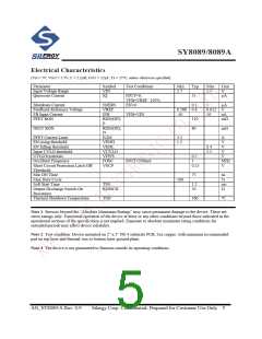
Electrical Characteristics
(VIN = 5V, VOUT = 2.5V, L = 2.2µH, COUT = 22µF, TA = 25°C, unless otherwise specified)
Parameter
Input Voltage Range
Quiescent Current
Symbol
VIN
IQ
Test Conditions
Min
2.7
Typ
55
Max
5.5
Unit
V
µA
IOUT=0,
VFB=VREF 105%
Shutdown Current
Feedback Reference Voltage
FB Input Current
ISHDN
VREF
IFB
RDS(ON),
P
EN=0
0.1
0.588 0.6
-50
1
µA
V
nA
mΩ
0.612
50
VFB=VIN
PFET RON
110
NFET RON
RDS(ON),
N
80
mΩ
PFET Current Limit
EN rising threshold
EN falling threshold
Input UVLO threshold
UVLO hysteresis
Oscillator Frequency
Short Circuit Protection Latch Off
Threshold
ILIM
3.5
1.5
A
V
V
V
V
MHz
V
VENH
VENL
VUVLO
VHYS
FOSC
VSCP
0.4
2.5
0.2
1
0.25
IOUT=500mA
Min ON Time
Max Duty Cycle
Soft Start Time
Output Discharge Switch On
Resistance
75
ns
%
ms
Ω
100
1.2
50
TSS
RDISCH
Thermal Shutdown Temperature
TSD
160
°C
Note 1: Stresses beyond the “Absolute Maximum Ratings” may cause permanent damage to the device. These are
stress ratings only. Functional operation of the device at these or any other conditions beyond those indicated in the
operational sections of the specification is not implied. Exposure to absolute maximum rating conditions for
extended periods may affect device reliability.
Note 2: Test condition: Device mounted on 2” x 2” FR-4 substrate PCB, 2oz copper, with minimum recommended
pad on top layer and thermal vias to bottom layer ground plane.
Note 3: The device is not guaranteed to function outside its operating conditions.
AN_SY8089/A Rev. 0.9
Silergy Corp. Confidential- Prepared for Customer Use Only 5

 SILICONIMAGE [ Silicon image ]