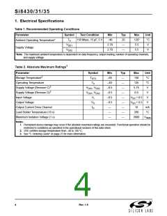
Si8430/31/35
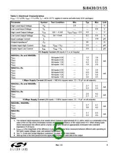
Table 3. Electrical Characteristics (Continued)
(VDD1 = 5 V ±10%, VDD2 = 5 V ±10%, TA = –40 to 125 ºC; applies to narrow and wide-body SOIC packages)
Parameter
Symbol
100 Mbps Supply Current (All inputs = 50 MHz square wave, CI = 15 pF on all outputs)
Si8430Bx, Si8435Bx
Test Condition
Min
Typ
Max
Unit
—
—
2.9
14.3
4.4
17.9
V
V
DD1
DD2
mA
mA
Si8431Bx
V
V
—
—
7.0
11.0
8.8
13.8
DD1
DD2
Timing Characteristics
Si843xAx
0
—
—
—
1.0
250
35
Mbps
ns
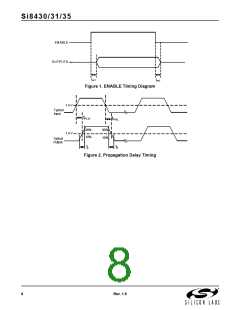
Maximum Data Rate
Minimum Pulse Width
Propagation Delay
—
—
t
, t
See Figure 2
See Figure 2
ns
PHL PLH
Pulse Width Distortion
PWD
—
—
25
ns
|t
- t
|
PLH PHL
2
t
—
—
—
—
40
35
ns
ns
Propagation Delay Skew
Channel-Channel Skew
Si843xBx
PSK(P-P)
t
PSK
0
—
—
150
6.0
9.5
Mbps
ns
Maximum Data Rate
Minimum Pulse Width
Propagation Delay
—
t
, t
See Figure 2
See Figure 2
3.0
6.0
ns
PHL PLH
Pulse Width Distortion
PWD
—
1.5
2.5
ns
|t
- t
|
PLH PHL
2
t
—
—
2.0
0.5
3.0
1.8
ns
ns
Propagation Delay Skew
PSK(P-P)
t
Channel-Channel Skew
PSK
Notes:
1. The nominal output impedance of an isolator driver channel is approximately 85 , ±40%, which is a combination of the
value of the on-chip series termination resistor and channel resistance of the output driver FET. When driving loads
where transmission line effects will be a factor, output pins should be appropriately terminated with controlled
impedance PCB traces.
2. tPSK(P-P) is the magnitude of the difference in propagation delay times measured between different units operating at
the same supply voltages, load, and ambient temperature.
3. See "3. Errata and Design Migration Guidelines" on page 25 for more details.
4. Start-up time is the time period from the application of power to valid data at the output.
6
Rev. 1.5

 SILICON [ SILICON ]