Si824x
3.4. Power Supply Connections
Isolation requirements mandate individual supplies for VDDI, VDDA, and VDDB. The decoupling caps for these
supplies must be placed as close to the VDD and GND pins of the Si824x as possible. The optimum values for
these capacitors depend on load current and the distance between the chip and the regulator that powers it. Low
effective series resistance (ESR) capacitors, such as Tantalum, are recommended.
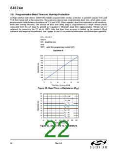
3.5. Power Dissipation Considerations
Proper system design must assure that the Si824x operates within safe thermal limits across the entire load range.
The Si824x total power dissipation is the sum of the power dissipated by bias supply current, internal switching
losses, and power delivered to the load. Equation 1 shows total Si824x power dissipation. In a non-overlapping
system, such as a high-side/low-side driver, n = 1.
PD = V
I
DDI DDI + 2V I
DDO QOUT + CintVDDO2F + 2nCLVDDO2F
where:
PD is the total Si824x device power dissipation (W)
IDDI is the input-side maximum bias current (3 mA)
IQOUT is the driver die maximum bias current (2.5 mA)
Cint is the internal parasitic capacitance (75 pF for the 0.5 A driver and 370 pF for the 4.0 A driver)
VDDI is the input-side VDD supply voltage (4.5 to 5.5 V)
VDDO is the driver-side supply voltage (10 to 24 V)
F is the switching frequency (Hz)
n is the overlap constant (max value = 2)
Equation 1.
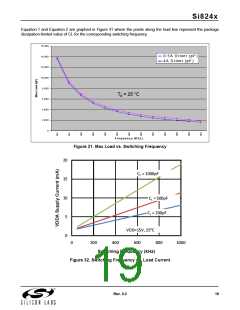
The maximum power dissipation allowable for the Si824x is a function of the package thermal resistance, ambient
temperature, and maximum allowable junction temperature, as shown in Equation 2:
T
jmax – TA
---------------------------
PDmax
where:
ja
PDmax = Maximum Si824x power dissipation (W)
Tjmax = Si824x maximum junction temperature (150 °C)
TA = Ambient temperature (°C)
ja = Si824x junction-to-air thermal resistance (105 °C/W)
F = Si824x switching frequency (Hz)
Equation 2.
Substituting values for P
T
, T , and into Equation 2 results in a maximum allowable total power
Dmax jmax A ja
dissipation of 1.19 W. Maximum allowable load is found by substituting this limit and the appropriate datasheet
values from Table 1 on page 5 into Equation 1 and simplifying. The result is Equation 3 (0.5 A driver) and
Equation 4 (4.0 A driver), both of which assume VDDI = 5 V and VDDA = VDDB = 18 V.
1.4 10–3
–11
--------------------------
CL(MAX)
=
– 7.5 10
F
Equation 3.
1.4 10–3
–10
--------------------------
CL(MAX)
=
– 3.7 10
F
Equation 4.
18
Rev. 0.2

 SILICON [ SILICON ]