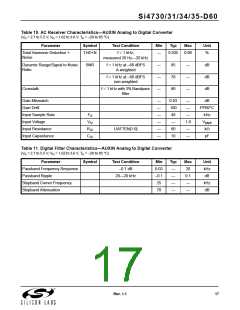
Si4730/31/34/35-D60
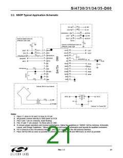
2.2. SSOP Typical Application Schematic
2
1
C7
C8
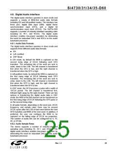
DFS
RIN
LIN
DOUT
R3
R2
R1
3
GP03/DCLK
LOUT
ROUT
DCLK
DFS
24
23
DOUT
Optional: Digital Audio Out
OPMODE: 0xB0, 0xB5
Si473x
C9
Optional: AUXIN/Digital Audio Out
OPMODE: 0x5B, 0x0B
C9
R1
R2
R3
1
24
DOUT
LOUT
DOUT
DFS
LOUT
ROUT
2
23
DFS
ROUT
3
22
GPO3/DCLK
GPO2/INT
DBYP
GPO3/DCLK
GPO2/INT
GPO1
C1
4
21
VA
2.0 to 5.5 V
VA
1.62 to 3.6 V
C4
5
20
19
18
17
16
15
14
13
GPO1
NC
VD
RCLK
SDIO
SCLK
SENB
VD
6
RCLK
SDIO
SCLK
SENB
RSTB
7
NC
C2
C3
8
FM Antenna
FMI
9
RFGND
NC
10
11
12
RSTB
GND
L1
NC
GND
AMI
Optional: AM Air Loop Antenna
L2
GPO3
RCLK
T1
C3
1
3
X1
AMI
C6
C5
RFGND
Optional: For Crystal OSC
Notes:
1. Place C1 close to VA and C4 close to VD pin.
2. All grounds connect directly to GND plane on PCB.
3. Pins 6 and 7 are no connects, leave floating.
4. Pins 10 and 11 are unused. Tie these pins to GND.
5. To ensure proper operation and receiver performance, follow the guidelines in “AN383: Si47xx Antenna, Schematic,
Layout, and Design Guidelines.” Silicon Laboratories will evaluate schematics and layouts for qualified customers.
6. Pin 8 connects to the FM antenna interface, and pin 12 connects to the AM antenna interface.
7. Place Si473x-D60 as close as possible to antenna and keep the FMI and AMI traces as short as possible.
Rev. 1.1
21

 SILICON [ SILICON ]