EFR32MG13 Mighty Gecko Multi-Protocol Wireless SoC Family Data Sheet
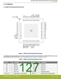
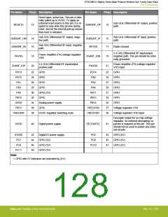
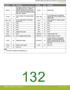
Pin Definitions
Pin Name
Pin(s) Description
Reset input, active low. This pin is inter-
Pin Name
Pin(s) Description
nally pulled up to AVDD. To apply an
external reset source to this pin, it is re-
quired to only drive this pin low during
reset, and let the internal pull-up ensure
that reset is released.
Sub GHz Differential RF output, positive
path.
RESETn
12
SUBGRF_OP
13
Sub GHz Differential RF output, nega-
tive path.
Sub GHz Differential RF input, positive
path.
SUBGRF_ON
SUBGRF_IN
14
16
SUBGRF_IP
RFVSS
15
17
Sub GHz Differential RF input, negative
path.
Radio Ground
2.4 GHz Differential RF input/output,
negative path. This pin should be exter-
nally grounded.
Power Amplifier (PA) voltage regulator
VSS
PAVSS
18
20
2G4RF_ION
PAVDD
19
21
2.4 GHz Differential RF input/output,
positive path.
Power Amplifier (PA) voltage regulator
VDD input
2G4RF_IOP
PD13
PD15
PA1
22
24
26
28
30
32
34
36
38
GPIO
PD14
PA0
23
25
27
29
31
33
35
37
39
GPIO
GPIO
GPIO
GPIO
PA2
GPIO
PA3
GPIO
PA4
GPIO
PA5
GPIO (5V)
PB11
GPIO
PB12
AVDD
PB15
VREGSW
GPIO
PB13
GPIO
Analog power supply.
GPIO
PB14
GPIO
VREGVSS
VREGVDD
Voltage regulator VSS
Voltage regulator VDD input
DCDC regulator switching node
Decouple output for on-chip voltage
regulator. An external decoupling ca-
pacitor is required at this pin. This pin
should not be used to power any exter-
nal circuits.
DVDD
40
Digital power supply.
DECOUPLE
41
IOVDD
PC7
42
44
46
48
Digital IO power supply.
GPIO (5V)
PC6
PC8
43
45
47
GPIO (5V)
GPIO (5V)
GPIO (5V)
PC9
GPIO (5V)
PC10
PC11
Note:
GPIO (5V)
1. GPIO with 5V tolerance are indicated by (5V).
silabs.com | Building a more connected world.
Rev. 1.4 | 128

 SILICON [ SILICON ]