EFM32G Data Sheet
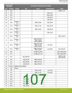
Pin Definitions
Alternate
LOCATION
Functionality
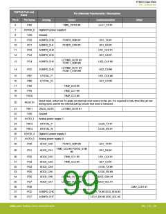
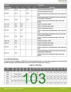
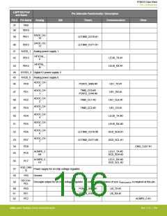
US0_CS
0
1
2
3
Description
PE13
PC8
USART0 chip select input / output.
USART0 Asynchronous Receive.
US0_RX
US0_TX
PE11
PE10
PC10
PC11
USART0 Synchronous mode Master Input / Slave Output (MI-
SO).
USART0 Asynchronous Transmit.Also used as receive input
in half duplex communication.
USART0 Synchronous mode Master Output / Slave Input
(MOSI).
US1_CLK
US1_CS
PB7
PB8
PD2
PD3
USART1 clock input / output.
USART1 chip select input / output.
USART1 Asynchronous Receive.
US1_RX
US1_TX
PC1
PC0
PD1
PD0
USART1 Synchronous mode Master Input / Slave Output (MI-
SO).
USART1 Asynchronous Transmit.Also used as receive input
in half duplex communication.
USART1 Synchronous mode Master Output / Slave Input
(MOSI).
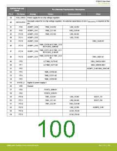
US2_CLK
US2_CS
PC4
PC5
USART2 clock input / output.
USART2 chip select input / output.
USART2 Asynchronous Receive.
US2_RX
US2_TX
PC3
PC2
USART2 Synchronous mode Master Input / Slave Output (MI-
SO).
USART2 Asynchronous Transmit.Also used as receive input
in half duplex communication.
USART2 Synchronous mode Master Output / Slave Input
(MOSI).
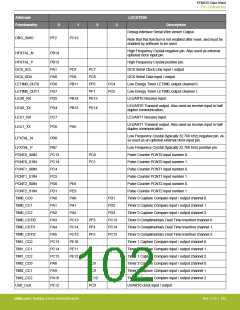
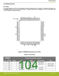
5.4.3 GPIO Pinout Overview
The specific GPIO pins available in EFM32G2322 is shown in the following table. Each GPIO port is organized as 16-bit ports indicated
by letters A through F, and the individual pin on this port is indicated by a number from 15 down to 0.
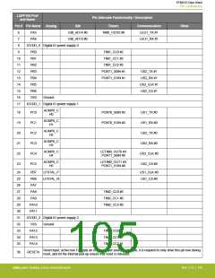
Table 5.12. GPIO Pinout
Port
Pin
15
Pin
14
Pin
13
Pin
12
Pin
11
Pin Pin 9 Pin 8 Pin 7 Pin 6 Pin 5 Pin 4 Pin 3 Pin 2 Pin 1 Pin 0
10
Port A
Port B
Port C
Port D
Port E
Port F
—
—
—
—
—
—
—
PA10 PA9 PA8
—
—
—
PA5 PA4 PA3 PA2 PA1 PA0
PB14 PB13
PB11
—
—
PB8 PB7
—
—
—
—
—
—
PC15 PC14 PC13 PC12 PC11 PC10 PC9 PC8 PC7 PC6 PC5 PC4 PC3 PC2 PC1 PC0
PD8 PD7 PD6 PD5 PD4 PD3 PD2 PD1 PD0
—
—
—
—
—
—
—
PE15 PE14 PE13 PE12 PE11 PE10 PE9 PE8
—
—
—
—
—
—
—
—
—
—
—
—
—
—
—
—
—
—
PF5 PF4 PF3 PF2 PF1 PF0
silabs.com | Building a more connected world.
Rev. 2.10 | 103

 SILICON [ SILICON ]