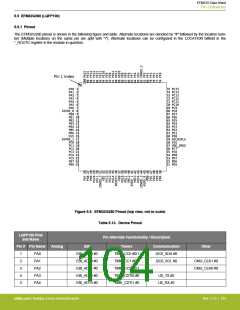
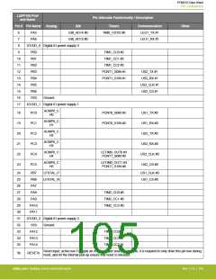
EFM32G Data Sheet
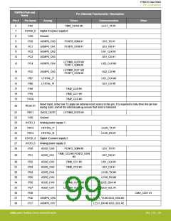
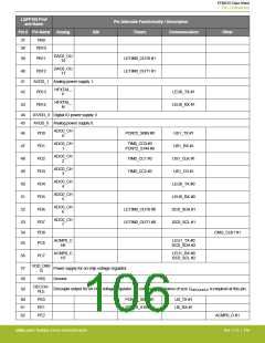
Pin Definitions
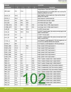
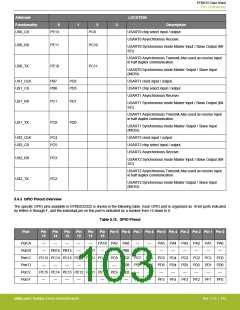
Alternate
LOCATION
Functionality
0
1
2
3
Description
Debug-interface Serial Wire viewer Output.
DBG_SWO
PF2
PC15
Note that this function is not enabled after reset, and must be
enabled by software to be used.
High Frequency Crystal negative pin. Also used as external
optional clock input pin.
HFXTAL_N
PB14
HFXTAL_P
I2C0_SCL
PB13
PA1
PA0
PD6
PD7
PD5
High Frequency Crystal positive pin.
I2C0 Serial Clock Line input / output.
I2C0 Serial Data input / output.
PD7
PD6
PB11
PC7
PC6
PF0
PF1
I2C0_SDA
LETIM0_OUT0
LETIM0_OUT1
LEU0_RX
PC4
PC5
Low Energy Timer LETIM0, output channel 0.
Low Energy Timer LETIM0, output channel 1.
LEUART0 Receive input.
PB14
PB13
PE15
PE14
LEUART0 Transmit output. Also used as receive input in half
duplex communication.
LEU0_TX
LEU1_RX
LEU1_TX
PD4
PC7
PC6
LEUART1 Receive input.
LEUART1 Transmit output. Also used as receive input in half
duplex communication.
PA5
Low Frequency Crystal (typically 32.768 kHz) negative pin. Al-
so used as an optional external clock input pin.
LFXTAL_N
PB8
LFXTAL_P
PCNT0_S0IN
PCNT0_S1IN
PCNT1_S0IN
PCNT1_S1IN
PCNT2_S0IN
PCNT2_S1IN
TIM0_CC0
PB7
Low Frequency Crystal (typically 32.768 kHz) positive pin.
Pulse Counter PCNT0 input number 0.
PC13
PC14
PC4
PC5
PD0
PD1
PA0
PC0
PC1
Pulse Counter PCNT0 input number 1.
Pulse Counter PCNT1 input number 0.
Pulse Counter PCNT1 input number 1.
PE8
Pulse Counter PCNT2 input number 0.
PE9
Pulse Counter PCNT2 input number 1.
PA0
PD1
PD2
PD3
Timer 0 Capture Compare input / output channel 0.
Timer 0 Capture Compare input / output channel 1.
Timer 0 Capture Compare input / output channel 2.
Timer 0 Complimentary Deat Time Insertion channel 0.
Timer 0 Complimentary Deat Time Insertion channel 1.
Timer 0 Complimentary Deat Time Insertion channel 2.
Timer 1 Capture Compare input / output channel 0.
Timer 1 Capture Compare input / output channel 1.
Timer 1 Capture Compare input / output channel 2.
Timer 2 Capture Compare input / output channel 0.
Timer 2 Capture Compare input / output channel 1.
Timer 2 Capture Compare input / output channel 2.
USART0 clock input / output.
TIM0_CC1
PA1
PA1
TIM0_CC2
PA2
PA2
TIM0_CDTI0
TIM0_CDTI1
TIM0_CDTI2
TIM1_CC0
PA3
PC13
PC14
PC15
PE10
PE11
PE12
PF3
PF4
PF5
PC13
PC14
PC15
PA4
PA5
PC13
PC14
PC15
PA8
TIM1_CC1
TIM1_CC2
TIM2_CC0
PC8
PC9
PC10
PC9
TIM2_CC1
PA9
TIM2_CC2
PA10
PE12
US0_CLK
silabs.com | Building a more connected world.
Rev. 2.10 | 102

 SILICON [ SILICON ]