C8051F52x-53x
1. System Overview
The C8051F52x/C8051F53x family of devices are fully integrated, very low power, mixed-signal system-
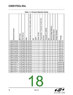
on-a-chip MCUs. Highlighted features are listed below. Refer to Table 1.1 for specific product feature
selection.
•
•
•
•
•
•
•
•
•
•
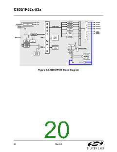
High-speed pipelined 8051-compatible microcontroller core (up to 25 MIPS)
In-system, full-speed, non-intrusive debug interface (on-chip)
True 12-bit 200 ksps ADC with analog multiplexer and up to 16 analog inputs
Precision programmable 24.5 MHz internal oscillator that is ±0.5% across voltage and temperature
Up to 7680 bytes of on-chip Flash memory
256 bytes of on-chip RAM
Enhanced UART, and SPI serial interfaces implemented in hardware
LIN 2.0 peripheral (V2.0 and V1.3 compatible, master and slave modes)
Three general-purpose 16-bit timers
Programmable Counter/Timer Array (PCA) with three capture/compare modules and Watchdog Timer
function
•
On-chip Power-On Reset, V Monitor, and Temperature Sensor
DD
•
•
On-chip Voltage Comparator
Up to 16 Port I/O
With on-chip Power-On Reset, V
monitor, Watchdog Timer, and clock oscillator, the C8051F52x/F53x
DD
devices are truly standalone system-on-a-chip solutions. The Flash memory is byte writable and can be
reprogrammed in-circuit, providing non-volatile data storage, and also allowing field upgrades of the 8051
firmware. User software has complete control of all peripherals, and may individually shut down any or all
peripherals for power savings.
The on-chip Silicon Laboratories 2-Wire (C2) Development Interface allows non-intrusive (uses no on-chip
resources), full speed, in-circuit debugging using the production MCU installed in the final application. This
debug logic supports inspection and modification of memory and registers, setting breakpoints, single
stepping, run and halt commands. All analog and digital peripherals are fully functional while debugging
using C2. The two C2 interface pins can be shared with user functions, allowing in-system programming
and debugging without occupying package pins.
Each device is specified for 2.7 to 5.25 V operation (supply voltage can be up to 5.25 V using on-chip reg-
ulator) over the automotive temperature range (–40 to +125 °C). The F52x is available in the QFN10
(3 x 3 mm) package. The F53x is available in the QFN20 (4 x 4 mm) or the TSSOP20 package.
Rev. 0.3
17

 SILICON [ SILICON ]