C8051F52x-53x
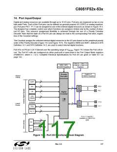
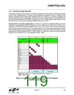
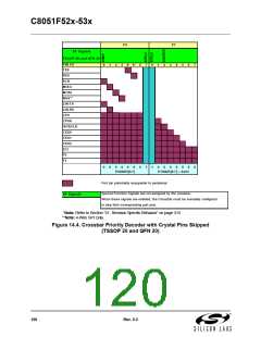
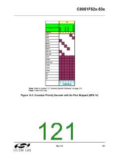
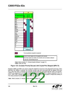
14.1. Priority Crossbar Decoder
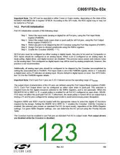
The Priority Crossbar Decoder (Figure 14.3) assigns a priority to each I/O function, starting at the top with
UART0. When a digital resource is selected, the least-significant unassigned Port pin is assigned to that
resource (excluding UART0, which will be assigned to pins P0.4 and P0.5). If a Port pin is assigned, the
Crossbar skips that pin when assigning the next selected resource. Additionally, the Crossbar will skip Port
pins whose associated bits in the PnSKIP registers are set. The PnSKIP registers allow software to skip
Port pins that are to be used for analog input, dedicated functions, or GPIO.
Important Note on Crossbar Configuration: If a Port pin is claimed by a peripheral without use of the
Crossbar, its corresponding PnSKIP bit should be set. This applies to P1.0 and/or P0.7 (‘F530) or P0.2
and/or P0.3 (‘F5250) for the external oscillator, P0.0 for V , P1.2 (‘F530) or P0.5 (‘F530) for the external
REF
CNVSTR signal, and any selected ADC or comparator inputs. The Crossbar skips selected pins as if they
were already assigned, and moves to the next unassigned pin. Figure 14.3 shows the Crossbar Decoder
priority with no Port pins skipped (P0SKIP, P1SKIP); Figure 14.4 shows the Crossbar Decoder priority with
the XTAL1 (P1.0) and XTAL2 (P1.1) pins skipped (P1SKIP = 0x03).
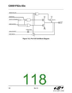
P 0
P 1
S F S igna ls
TS S OP 20 a nd QFN 20
P IN I/O
0
1
2
3
4* 5*
6
7
0
1
2
3
4
5
6
7
TX 0
RX 0
S CK
M IS O
M OS I
NS S **
LIN-TX
LIN_RX
CP 0
CP 0A
/S YS CLK
CEX 0
CEX 1
CEX 2
ECI
T0
T1
0
0
0
0
0
0
0
0
0
0
0
0
0
0
0
0
P 0S KIP [0:7]
P 1S KIP [0:7]
*Note: Refer to Section “21. Revision Specific Behavior” on page 215.
**Note: 4-Wire SPI Only.
Figure 14.3. Crossbar Priority Decoder with No Pins Skipped
(TSSOP 20 and QFN 20)
Rev. 0.3
119

 SILICON [ SILICON ]